
“Architecture and Programming of 8051 Microcontrollers”
 Learn in a quick and easy way to program 8051 microcontroller using many practical examples we have provided for you. Despite its relative old age, 8051 is still the most commonly used microcontroller at present. Beside Intel, many other renowned companies manufacture this model - Philips, Siemens, etc. The book contains details of its architecture and many practical examples, both simple and complex, useful program routines, instructions on handling the programmer for Atmel 51 series, and the guide on using the development systems for Atmel microcontrollers. In the appendices you will find detailed assembler instructions with examples, glossary and much more...
Table of Contents
- Chapter 1: Introduction to Microcontrollers
- Chapter 2: 8051 Microcontroller Architecture
- Chapter 3: The 8051 Instruction Set
- Chapter 4: The AT89S8253 Microcontroller
- Chapter 5: Program Language Assembler
- Chapter 6: Examples
- Chapter 7: Development Tools
- Chapter 8: Other Resources
- Chapter1
- Chapter2
- Chapter3
- Chapter4
- Chapter5
- Chapter6
- Chapter7
- Chapter8
Chapter1: Introduction to Microcontrollers
- Introduction
- 1.1 What are microcontrollers and what are they used for?
- 1.2 What is what in microcontroller?
Introduction
It was electricity in the beginning....The people were happy because they did not know that it was all around them and could be utilized. That was good. Then Faraday came and a stone has started to roll slowly...
The first machines using a new sort of energy appeared soon. A long time has passed since then and just when the people finally got used to them and stopped paying attention to what a new generation of specialists were doing, someone came to an idea that electrons could be a very convenient toy being closed in a glass pipe. It was just a good idea at first, but there was no return. Electonics was born and the stone kept on rolling down the hill faster and faster...
A new science - new specialists. Blue coats were replaced with white ones and people who knew something about electronics appeared on the stage. While the rest of humanity were passively watching in disbelief what was going on, the plotters split in two groups - “software-oriented” and “hardware-oriented”. Somewhat younger than their teachers, very enthusiastic and full of ideas, both of them kept on working but separate ways. While the first group was developing constantly and gradually, the hardware-oriented people, driven by success, threw caution to the wind and invented transistors.
Up till that moment, the things could be more or less kept under control, but a broad publicity was not aware of what was going on, which soon led to a fatal mistake! Being naive in belief that cheap tricks could slow down technology development and development of the world and retrieve the good all days, mass market opened its doors for the products of Electronics Industry, thus closing a magic circle. A rapid drop in prices made these components available for a great variety of people. The stone was falling freely...
The first integrated circuits and processors appeared soon, which caused computers and other products of electronics to drop down in price even more. They could be bought everywhere. Another circle was closed! Ordinary people got hold of computers and computer era has begun...
While this drama was going on, hobbyists and professionals, also split in two groups and protected by anonymity, were working hard on their projects. Then, someone suddenly put a question: Why should not we make a universal component? A cheap, universal integrated circuit that could be programmed and used in any field of electronics, device or wherever needed? Technology has been developed enough as well as the market. Why not? So it happened, body and spirit were united and the first integrated circuit was designed and called the MICROCONTROLLER.
1.1 What are microcontrollers and what are they used for?
Like all good things, this powerful component is basically very simple. It is made by mixing tested and high- quality "ingredients" (components) as per following receipt:
- The simplest computer processor is used as the "brain" of the future system.
- Depending on the taste of the manufacturer, a bit of memory, a few A/D converters, timers, input/output lines etc. are added
- All that is placed in some of the standard packages.
- A simple software able to control it all and which everyone can easily learn about has been developed.
On the basis of these rules, numerous types of microcontrollers were designed and they quickly became man's invisible companion. Their incredible simplicity and flexibility conquered us a long time ago and if you try to invent something about them, you should know that you are probably late, someone before you has either done it or at least has tried to do it.
The following things have had a crucial influence on development and success of the microcontrollers:
- Powerful and carefully chosen electronics embedded in the microcontrollers can independetly or via input/output devices (switches, push buttons, sensors, LCD displays, relays etc.), control various processes and devices such as industrial automation, electric current, temperature, engine performance etc.
- Very low prices enable them to be embedded in such devices in which, until recent time it was not worthwhile to embed anything. Thanks to that, the world is overwhelmed today with cheap automatic devices and various “smart” appliences.
- Prior knowledge is hardly needed for programming. It is sufficient to have a PC (software in use is not demanding at all and is easy to learn) and a simple device (called the programmer) used for “loading” raedy-to-use programs into the microcontroller.
So, if you are infected with a virus called electronics, there is nothing left for you to do but to learn how to use and control its power
How does the microcontroller operate?
Even though there is a large number of different types of microcontrollers and even more programs created for their use only, all of them have many things in common. Thus, if you learn to handle one of them you will be able to handle them all. A typical scenario on the basis of which it all functions is as follows:
- Power supply is turned off and everything is still…the program is loaded into the microcontroller, nothing indicates what is about to come…
- Power supply is turned on and everything starts to happen at high speed! The control logic unit keeps everything under control. It disables all other circuits except quartz crystal to operate. While the preparations are in progress, the first milliseconds go by.
- Power supply voltage reaches its maximum and oscillator frequency becomes stable. SFRs are being filled with bits reflecting the state of all circuits within the microcontroller. All pins are configured as inputs. The overall electronis starts operation in rhythm with pulse sequence. From now on the time is measured in micro and nanoseconds.
- Program Counter is set to zero. Instruction from that address is sent to instruction decoder which recognizes it, after which it is executed with immediate effect.
- The value of the Program Counter is incremented by 1 and the whole process is repeated...several million times per second.
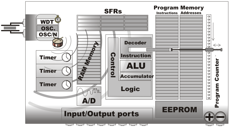
1.2 What is what in the microcontroller?
As you can see, all the operations within the microcontroller are performed at high speed and quite simply, but the microcontroller itself would not be so useful if there are not special circuits which make it complete. In continuation, we are going to call your attention to them.
Read Only Memory (ROM)
Read Only Memory (ROM) is a type of memory used to permanently save the program being executed. The size of the program that can be written depends on the size of this memory. ROM can be built in the microcontroller or added as an external chip, which depends on the type of the microcontroller. Both options have some disadvantages. If ROM is added as an external chip, the microcontroller is cheaper and the program can be considerably longer. At the same time, a number of available pins is reduced as the microcontroller uses its own input/output ports for connection to the chip. The internal ROM is usually smaller and more expensive, but leaves more pins available for connecting to peripheral environment. The size of ROM ranges from 512B to 64KB.
Random Access Memory (RAM)
Random Access Memory (RAM) is a type of memory used for temporary storing data and intermediate results created and used during the operation of the microcontrollers. The content of this memory is cleared once the power supply is off. For example, if the program performes an addition, it is necessary to have a register standing for what in everyday life is called the “sum” . For that purpose, one of the registers in RAM is called the "sum" and used for storing results of addition. The size of RAM goes up to a few KBs.
Electrically Erasable Programmable ROM (EEPROM)
The EEPROM is a special type of memory not contained in all microcontrollers. Its contents may be changed during program execution (similar to RAM ), but remains permanently saved even after the loss of power (similar to ROM). It is often used to store values, created and used during operation (such as calibration values, codes, values to count up to etc.), which must be saved after turning the power supply off. A disadvantage of this memory is that the process of programming is relatively slow. It is measured in miliseconds.
Special Function Registers (SFR)
 Special function registers are part of RAM memory. Their purpose is predefined by the manufacturer and cannot be changed therefore. Since their bits are physically connected to particular circuits within the microcontroller, such as A/D converter, serial communication module etc., any change of their state directly affects the operation of the microcontroller or some of the circuits. For example, writing zero or one to the SFR controlling an input/output port causes the appropriate port pin to be configured as input or output. In other words, each bit of this register controls the function of one single pin.
Program Counter
Program Counter is an engine running the program and points to the memory address containing the next instruction to execute. After each instruction execution, the value of the counter is incremented by 1. For this reason, the program executes only one instruction at a time just as it is written. However…the value of the program counter can be changed at any moment, which causes a “jump” to a new memory location. This is how subroutines and branch instructions are executed. After jumping, the counter resumes even and monotonous automatic counting +1, +1, +1…
Central Processor Unit (CPU)
As its name suggests, this is a unit which monitors and controls all processes within the microcontroller and the user cannot affect its work. It consists of several smaller subunits, of which the most important are:
- Instruction decoder is a part of the electronics which recognizes program instructions and runs other circuits on the basis of that. The abilities of this circuit are expressed in the "instruction set" which is different for each microcontroller family.
- Arithmetical Logical Unit (ALU) performs all mathematical and logical operations upon data.
- Accumulator is an SFR closely related to the operation of ALU. It is a kind of working desk used for storing all data upon which some operations should be executed (addition, shift etc.). It also stores the results ready for use in further processing. One of the SFRs, called the Status Register, is closely related to the accumulator, showing at any given time the "status" of a number stored in the accumulator (the number is greater or less than zero etc.).
![]()
A bit is just a word invented to confuse novices at electronics. Joking aside, this word in practice indicates whether the voltage is present on a conductor or not. If it is present, the approprite pin is set to logic one (1), i.e. the bit’s value is 1. Otherwise, if the voltage is 0 V, the appropriate pin is cleared (0), i.e. the bit’s value is 0. It is more complicated in theory where a bit is referred to as a binary digit, but even in this case, its value can be either 0 or 1.
Input/output ports (I/O Ports)
In order to make the microcontroller useful, it is necessary to connect it to peripheral devices. Each microcontroller has one or more registers (called a port) connected to the microcontroller pins. Why do we call them input/output ports? Because it is possible to change a pin function according to the user's needs. These registers are the only registers in the microcontroller the state of which can be checked by voltmeter!
Oscillator
 Even pulses generated by the oscillator enable harmonic and synchronous operation of all circuits within the microcontroller. It is usually configured as to use quartz-crystal or ceramics resonator for frequency stabilization. It can also operate without elements for frequency stabilization (like RC oscillator). It is important to say that program instructions are not executed at the rate imposed by the oscillator itself, but several times slower. It happens because each instruction is executed in several steps. For some microcontrollers, the same number of cycles is needed to execute any instruction, while it's different for other microcontrollers. Accordingly, if the system uses quartz crystal with a frequency of 20MHz, the execution time of an instruction is not expected 50nS, but 200, 400 or even 800 nS, depending on the type of the microcontroller!
Timers/Counters
Most programs use these miniature electronic "stopwatches" in their operation. These are commonly 8- or 16-bit SFRs the contents of which is automatically incremented by each coming pulse. Once the register is completely loaded, an interrupt is generated!
If these registers use an internal quartz oscillator as a clock source, then it is possible to measure the time between two events (if the register value is T1 at the moment measurement has started, and T2 at the moment it has finished, then the elapsed time is equal to the result of subtraction T2-T1 ). If the registers use pulses coming from external source, then such a timer is turned into a counter.
 This is only a simple explanation of the operation itself. It’s somehow more complicated in practice.

A register or a memory cell is an electronic circuit which can memorize the state of one byte. Besides 8 bits available to the user, each register has also a number of addressing bits. It is important to remember that:
- All registers of ROM as well as those of RAM referred to as general-purpose registers are mutually equal and nameless. During programming, each of them can be assigned a name, which makes the whole operation much easier.
- All SFRs are assigned names which are different for different types of the microcontrollers and each of them has a special function as their name suggests.
Watchdog timer
The Watchdog Timer is a timer connected to a completely separate RC oscillator within the microcontroller.
If the watchdog timer is enabled, every time it counts up to the program end, the microcontroller reset occurs and program execution starts from the first instruction. The point is to prevent this from happening by using a special command. The whole idea is based on the fact that every program is executed in several longer or shorter loops.
If instructions resetting the watchdog timer are set at the appropriate program locations, besides commands being regularly executed, then the operation of the watchdog timer will not affect the program execution.
If for any reason (usually electrical noise in industry), the program counter "gets stuck" at some memory location from which there is no return, the watchdog will not be cleared, so the register’s value being constantly incremented will reach the maximum et voila! Reset occurs!
Power Supply Circuit
There are two things worth attention concerning the microcontroller power supply circuit:
 Brown out is a potentially dangerous state which occurs at the moment the microcontroller is being turned off or when power supply voltage drops to the lowest level due to electric noise. As the microcontroller consists of several circuits which have different operating voltage levels, this can cause its out of control performance. In order to prevent it, the microcontroller usually has a circuit for brown out reset built-in. This circuit immediately resets the whole electronics when the voltage level drops below the lower limit.
Reset pin is usually referred to as Master Clear Reset (MCLR) and serves for external reset of the microcontroller by applying logic zero (0) or one (1) depending on the type of the microcontroller. In case the brown out is not built in the microcontroller, a simple external circuit for brown out reset can be connected to this pin.
Serial communication
 Parallel connections between the microcontroller and peripherals established over I/O ports are the ideal solution for shorter distances up to several meters. However, in other cases, when it is necessary to establish communication between two devices on longer distances it is obviously not possible to use parallel connections. Then, serial communication is the best solution.
Today, most microcontrollers have several different systems for serial communication built in as a standard equipment. Which of them will be used depends on many factors of which the most important are:
- How many devices the microcontroller has to exchange data with?
- How fast the data exchange has to be?
- What is the distance between devices?
- Is it necessary to send and receive data simultaneously?
One of the most important things concerning serial communication is the Protocol which should be strictly observed. It is a set of rules which must be applied in order that devices can correctly interpret data they mutually exchange. Fortunately, the microcontrollers automatically take care of this, so the work of the programmer/user is reduced to a simple write (data to be sent) and read (received data).
![]()
A byte consists of 8 bits grouped together. If a bit is a digit then it is logical that bytes are numbers. All mathematical operations can be performed upon them, just like upon common decimal numbers, which is carried out in the ALU. It is important to remember that byte digits are not of equal significance. The largest value has the leftmost bit called the most significant bit (MSB). The rightmost bit has the least value and is therefore called the least significant bit (LSB). Since 8 digits (zeros and ones) of one byte can be combined in 256 different ways, the largest decimal number which can be represented by one byte is 255 (one combination represents zero).
Program
Unlike other integrated circuits which only need to be connected to other components and turn the power supply on, the microcontrollers need to be programmed first. This is a so called "bitter pill" and the main reason why hardware-oriented electronics engineers stay away from microcontrollers. It is a trap causing huge losses because the process of programming the microcontroller is basically very simple.
In order to write a program for the microcontroller, several "low-level" programming languages can be used such as Assembly, C and Basic (and their versions as well). Writing program procedure consists of simple writing instructions in the order in which they should be executed. There are also many programs running in Windows environment used to facilitate the work providing additional visual tools.
This book describes the use of Assembly because it is the simplest language with the fastest execution allowing entire control on what is going on in the circuit.
![]()
Interrupt - electronics is usually more faster than physical processes it should keep under control. This is why the microcontroller spends most of its time waiting for something to happen or execute. In other words, when some event takes place, the microcontroller does something. In order to prevent the microcontroller from spending most of its time endlessly checking for logic state on input pins and registers, an interrupt is generated. It is the signal which informs the central processor that something attention worthy has happened. As its name suggests, it interrupts regular program execution. It can be generated by different sources so when it occurs, the microcontroller immediately stops operation and checks for the cause. If it is needed to perform some operations, a current state of the program counter is pushed onto the Stack and the appropriate program is executed. It's the so called interrupt routine.
Stack is a part of RAM used for storing the current state of the program counter (address) when an interrupt occurs. In this way, after a subroutine or an interrupt execution, the microcontroller knows from where to continue regular program execution. This address is cleared after returning to the program because there is no need to save it any longer, and one location of the stack is automatically availale for further use. In addition, the stack can consist of several levels. This enables subroutines’ nesting, i.e. calling one subroutine from another.
Chapter 2 : 8051 Microcontroller Architecture
- 2.1 What is 8051 Standard?
- 2.2 8051 Microcontroller's pins
- 2.3 Input/Output Ports (I/O Ports)
- 2.4 8051 Microcontroller Memory Organisation
- 2.5 SFRs (Special Function Registers)
- 2.6 Counters and Timers
- 2.7 UART (Universal Asynchronous Receiver and Transmitter)
- 2.8 8051 Microcontroller Interrupts
- 2.9 8051 Microcontroller Power Consumption Control
2.1 What is 8051 Standard?
Microcontroller manufacturers have been competing for a long time for attracting choosy customers and every couple of days a new chip with a higher operating frequency, more memory and upgraded A/D converters appeared on the market.
However, most of them had the same or at least very similar architecture known in the world of microcontrollers as “8051 compatible”. What is all this about?
The whole story has its beginnings in the far 80s when Intel launched the first series of microcontrollers called the MCS 051. Even though these microcontrollers had quite modest features in comparison to the new ones, they conquered the world very soon and became a standard for what nowadays is called the microcontroller.
The main reason for their great success and popularity is a skillfully chosen configuration which satisfies different needs of a large number of users allowing at the same time constant expansions (refers to the new types of microcontrollers). Besides, the software has been developed in great extend in the meantime, and it simply was not profitable to change anything in the microcontroller’s basic core. This is the reason for having a great number of various microcontrollers which basically are solely upgraded versions of the 8051 family. What makes this microcontroller so special and universal so that almost all manufacturers all over the world manufacture it today under different name?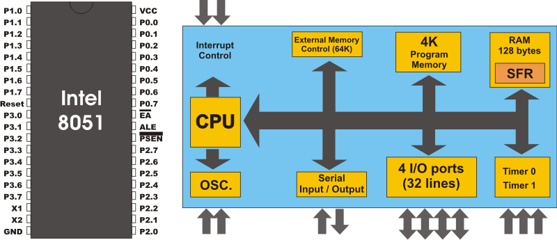 As seen in figure above, the 8051 microcontroller has nothing impressive in appearance:
- 4 Kb of ROM is not much at all.
- 128b of RAM (including SFRs) satisfies the user's basic needs.
- 4 ports having in total of 32 input/output lines are in most cases sufficient to make all necessary connections to peripheral environment.
The whole configuration is obviously thought of as to satisfy the needs of most programmers working on development of automation devices. One of its advantages is that nothing is missing and nothing is too much. In other words, it is created exactly in accordance to the average user‘s taste and needs. Another advantages are RAM organization, the operation of Central Processor Unit (CPU) and ports which completely use all recourses and enable further upgrade.
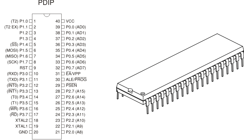
2.2 Pinout Description
Pins 1-8: Port 1 Each of these pins can be configured as an input or an output.
Pin 9: RS A logic one on this pin disables the microcontroller and clears the contents of most registers. In other words, the positive voltage on this pin resets the microcontroller. By applying logic zero to this pin, the program starts execution from the beginning.
Pins10-17: Port 3 Similar to port 1, each of these pins can serve as general input or output. Besides, all of them have alternative functions:
Pin 10: RXD Serial asynchronous communication input or Serial synchronous communication output.
Pin 11: TXD Serial asynchronous communication output or Serial synchronous communication clock output.
Pin 12: INT0 Interrupt 0 input.
Pin 13: INT1 Interrupt 1 input.
Pin 14: T0 Counter 0 clock input.
Pin 15: T1 Counter 1 clock input.
Pin 16: WR Write to external (additional) RAM.
Pin 17: RD Read from external RAM.
Pin 18, 19: X2, X1 Internal oscillator input and output. A quartz crystal which specifies operating frequency is usually connected to these pins. Instead of it, miniature ceramics resonators can also be used for frequency stability. Later versions of microcontrollers operate at a frequency of 0 Hz up to over 50 Hz.
Pin 20: GND Ground.
Pin 21-28: Port 2 If there is no intention to use external memory then these port pins are configured as general inputs/outputs. In case external memory is used, the higher address byte, i.e. addresses A8-A15 will appear on this port. Even though memory with capacity of 64Kb is not used, which means that not all eight port bits are used for its addressing, the rest of them are not available as inputs/outputs.
Pin 29: PSEN If external ROM is used for storing program then a logic zero (0) appears on it every time the microcontroller reads a byte from memory.
Pin 30: ALE Prior to reading from external memory, the microcontroller puts the lower address byte (A0-A7) on P0 and activates the ALE output. After receiving signal from the ALE pin, the external register (usually 74HCT373 or 74HCT375 add-on chip) memorizes the state of P0 and uses it as a memory chip address. Immediately after that, the ALU pin is returned its previous logic state and P0 is now used as a Data Bus. As seen, port data multiplexing is performed by means of only one additional (and cheap) integrated circuit. In other words, this port is used for both data and address transmission.
Pin 31: EA By applying logic zero to this pin, P2 and P3 are used for data and address transmission with no regard to whether there is internal memory or not. It means that even there is a program written to the microcontroller, it will not be executed. Instead, the program written to external ROM will be executed. By applying logic one to the EA pin, the microcontroller will use both memories, first internal then external (if exists).
Pin 32-39: Port 0 Similar to P2, if external memory is not used, these pins can be used as general inputs/outputs. Otherwise, P0 is configured as address output (A0-A7) when the ALE pin is driven high (1) or as data output (Data Bus) when the ALE pin is driven low (0).
Pin 40: VCC +5V power supply.
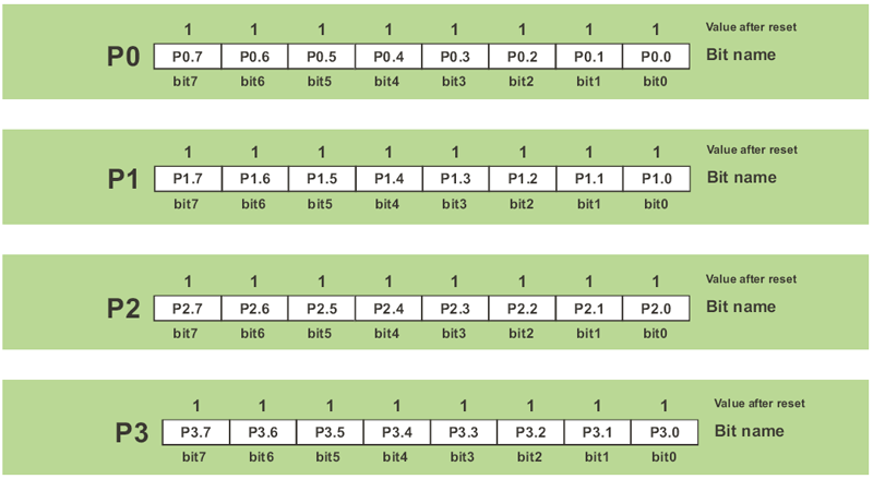
2.3 Input/Output Ports (I/O Ports)
All 8051 microcontrollers have 4 I/O ports each comprising 8 bits which can be configured as inputs or outputs. Accordingly, in total of 32 input/output pins enabling the microcontroller to be connected to peripheral devices are available for use.
Pin configuration, i.e. whether it is to be configured as an input (1) or an output (0), depends on its logic state. In order to configure a microcontroller pin as an input, it is necessary to apply a logic zero (0) to appropriate I/O port bit. In this case, voltage level on appropriate pin will be 0.
Similarly, in order to configure a microcontroller pin as an input, it is necessary to apply a logic one (1) to appropriate port. In this case, voltage level on appropriate pin will be 5V (as is the case with any TTL input). This may seem confusing but don't loose your patience. It all becomes clear after studying simple electronic circuits connected to an I/O pin.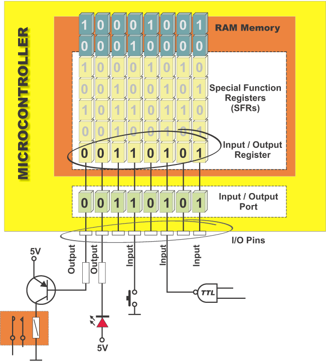
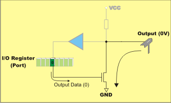
Input/Output (I/O) pin Figure above illustrates a simplified schematic of all circuits within the microcontroler connected to one of its pins. It refers to all the pins except those of the P0 port which do not have pull-up resistors built-in. |
Output pin A logic zero (0) is applied to a bit of the P register. The output FE transistor is turned on, thus connecting the appropriate pin to ground.
|

Input pin A logic one (1) is applied to a bit of the P register. The output FE transistor is turned off and the appropriate pin remains connected to the power supply voltage over a pull-up resistor of high resistance. |
Port 0
The P0 port is characterized by two functions. If external memory is used then the lower address byte (addresses A0-A7) is applied on it. Otherwise, all bits of this port are configured as inputs/outputs.
The other function is expressed when it is configured as an output. Unlike other ports consisting of pins with built-in pull-up resistor connected by its end to 5 V power supply, pins of this port have this resistor left out. This apparently small difference has its consequences:
If any pin of this port is configured as an input then it acts as if it “floats”. Such an input has unlimited input resistance and indetermined potential.

When the pin is configured as an output, it acts as an “open drain”. By applying logic 0 to a port bit, the appropriate pin will be connected to ground (0V). By applying logic 1, the external output will keep on “floating”. In order to apply logic 1 (5V) on this output pin, it is necessary to built in an external pull-up resistor.
Port 1
P1 is a true I/O port, because it doesn't have any alternative functions as is the case with P0, but can be cofigured as general I/O only. It has a pull-up resistor built-in and is completely compatible with TTL circuits.
Port 2
P2 acts similarly to P0 when external memory is used. Pins of this port occupy addresses intended for external memory chip. This time it is about the higher address byte with addresses A8-A15. When no memory is added, this port can be used as a general input/output port showing features similar to P1.
Port 3
All port pins can be used as general I/O, but they also have an alternative function. In order to use these alternative functions, a logic one (1) must be applied to appropriate bit of the P3 register. In tems of hardware, this port is similar to P0, with the difference that its pins have a pull-up resistor built-in.
Pin's Current limitations
When configured as outputs (logic zero (0)), single port pins can receive a current of 10mA. If all 8 bits of a port are active, a total current must be limited to 15mA (port P0: 26mA). If all ports (32 bits) are active, total maximum current must be limited to 71mA. When these pins are configured as inputs (logic 1), built-in pull-up resistors provide very weak current, but strong enough to activate up to 4 TTL inputs of LS series.
2.4 Memory Organization
The 8051 has two types of memory and these are Program Memory and Data Memory. Program Memory (ROM) is used to permanently save the program being executed, while Data Memory (RAM) is used for temporarily storing data and intermediate results created and used during the operation of the microcontroller. Depending on the model in use (we are still talking about the 8051 microcontroller family in general) at most a few Kb of ROM and 128 or 256 bytes of RAM is used. However…
All 8051 microcontrollers have a 16-bit addressing bus and are capable of addressing 64 kb memory. It is neither a mistake nor a big ambition of engineers who were working on basic core development. It is a matter of smart memory organization which makes these microcontrollers a real “programmers’ goody“.
Program MemoryThe first models of the 8051 microcontroller family did not have internal program memory. It was added as an external separate chip. These models are recognizable by their label beginning with 803 (for example 8031 or 8032). All later models have a few Kbyte ROM embedded. Even though such an amount of memory is sufficient for writing most of the programs, there are situations when it is necessary to use additional memory as well. A typical example are so called lookup tables. They are used in cases when equations describing some processes are too complicated or when there is no time for solving them. In such cases all necessary estimates and approximates are executed in advance and the final results are put in the tables (similar to logarithmic tables).
How does the microcontroller handle external memory depends on the EA pin logic state:

EA=0 In this case, the microcontroller completely ignores internal program memory and executes only the program stored in external memory.
EA=1 In this case, the microcontroller executes first the program from built-in ROM, then the program stored in external memory.
In both cases, P0 and P2 are not available for use since being used for data and address transmission. Besides, the ALE and PSEN pins are also used.
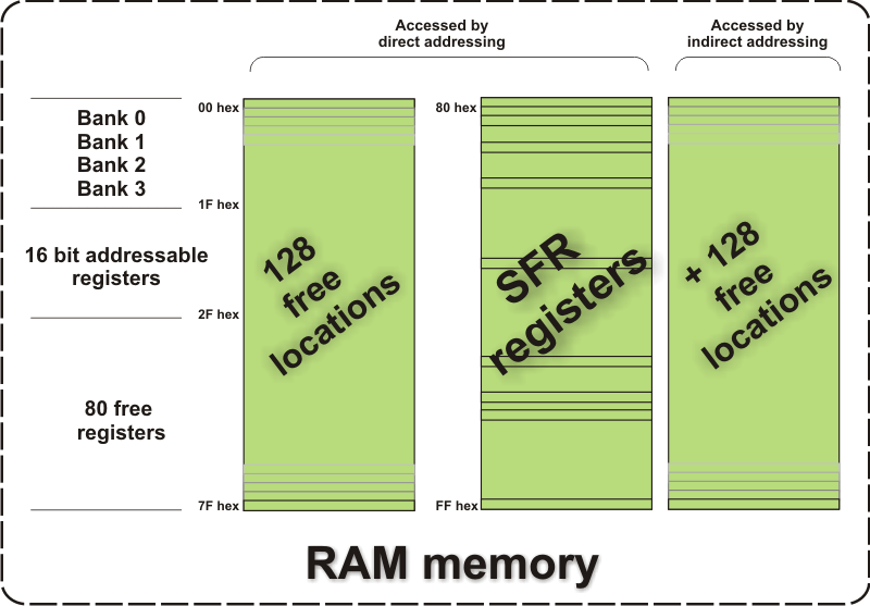
Data MemoryAs already mentioned, Data Memory is used for temporarily storing data and intermediate results created and used during the operation of the microcontroller. Besides, RAM memory built in the 8051 family includes many registers such as hardware counters and timers, input/output ports, serial data buffers etc. The previous models had 256 RAM locations, while for the later models this number was incremented by additional 128 registers. However, the first 256 memory locations (addresses 0-FFh) are the heart of memory common to all the models belonging to the 8051 family. Locations available to the user occupy memory space with addresses 0-7Fh, i.e. first 128 registers. This part of RAM is divided in several blocks.
The first block consists of 4 banks each including 8 registers denoted by R0-R7. Prior to accessing any of these registers, it is necessary to select the bank containing it. The next memory block (address 20h-2Fh) is bit- addressable, which means that each bit has its own address (0-7Fh). Since there are 16 such registers, this block contains in total of 128 bits with separate addresses (address of bit 0 of the 20h byte is 0, while address of bit 7 of the 2Fh byte is 7Fh). The third group of registers occupy addresses 2Fh-7Fh, i.e. 80 locations, and does not have any special functions or features.
Additional RAMIn order to satisfy the programmers’ constant hunger for Data Memory, the manufacturers decided to embed an additional memory block of 128 locations into the latest versions of the 8051 microcontrollers. However, it’s not as simple as it seems to be… The problem is that electronics performing addressing has 1 byte (8 bits) on disposal and is capable of reaching only the first 256 locations, therefore. In order to keep already existing 8-bit architecture and compatibility with other existing models a small trick was done.
What does it mean? It means that additional memory block shares the same addresses with locations intended for the SFRs (80h- FFh). In order to differentiate between these two physically separated memory spaces, different ways of addressing are used. The SFRs memory locations are accessed by direct addressing, while additional RAM memory locations are accessed by indirect addressing.

Memory expansion
In case memory (RAM or ROM) built in the microcontroller is not sufficient, it is possible to add two external memory chips with capacity of 64Kb each. P2 and P3 I/O ports are used for their addressing and data transmission.

From the user’s point of view, everything works quite simply when properly connected because most operations are performed by the microcontroller itself. The 8051 microcontroller has two pins for data read RD#(P3.7) and PSEN#. The first one is used for reading data from external data memory (RAM), while the other is used for reading data from external program memory (ROM). Both pins are active low. A typical example of memory expansion by adding RAM and ROM chips (Hardward architecture), is shown in figure above.
Even though additional memory is rarely used with the latest versions of the microcontrollers, we will describe in short what happens when memory chips are connected according to the previous schematic. The whole process described below is performed automatically.
- When the program during execution encounters an instruction which resides in external memory (ROM), the microcontroller will activate its control output ALE and set the first 8 bits of address (A0-A7) on P0. IC circuit 74HCT573 passes the first 8 bits to memory address pins.
- A signal on the ALE pin latches the IC circuit 74HCT573 and immediately afterwards 8 higher bits of address (A8-A15) appear on the port. In this way, a desired location of additional program memory is addressed. It is left over to read its content.
- Port P0 pins are configured as inputs, the PSEN pin is activated and the microcontroller reads from memory chip.
Similar occurs when it is necessary to read location from external RAM. Addressing is performed in the same way, while read and write are performed via signals appearing on the control outputs RD (is short for read) or WR (is short for write).
AddressingWhile operating, the processor processes data as per program instructions. Each instruction consists of two parts. One part describes WHAT should be done, while the other explains HOW to do it. The latter part can be a data (binary number) or the address at which the data is stored. Two ways of addressing are used for all 8051 microcontrollers depending on which part of memory should be accessed:
Direct AddressingOn direct addressing, the address of memory location containing data to be read is specified in instruction. The address may contain a number being changed during operation (variable). For example:
Since the address is only one byte in size (the largest number is 255), only the first 255 locations of RAM can be accessed this way. The first half of RAM is available for use, while another half is reserved for SFRs.
MOV A,33h; Means: move a number from address 33 hex. to accumulatorIndirect Addressing
On indirect addressing, a register containing the address of another register is specified in instruction. Data to be used in the program is stored in the letter register. For example:
Indirect addressing is only used for accessing RAM locations available for use (never for accessing SFRs). This is the only way of accessing all the latest versions of the microcontrollers with additional memory block (128 locations of RAM). Simply put, when the program encounters instruction including “@” sign and if the specified address is higher than 128 ( 7F hex.), the processor knows that indirect addressing is used and skips memory space reserved for SFRs.
MOV A,@R0; Means: Store the value from the register whose address is in the R0 register into accumulator
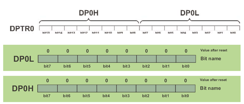
On indirect addressing, registers R0, R1 or Stack Pointer are used for specifying 8-bit addresses. Since only 8 bits are avilable, it is possible to access only registers of internal RAM this way (128 locations when speaking of previous models or 256 locations when speaking of latest models of microcontrollers). If an extra memory chip is added then the 16-bit DPTR Register (consisting of the registers DPTRL and DPTRH) is used for specifying address. In this way it is possible to access any location in the range of 64K.
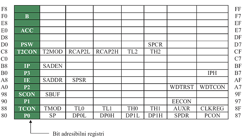
2.5 Special Function Registers (SFRs)
Special Function Registers (SFRs) are a sort of control table used for running and monitoring the operation of the microcontroller. Each of these registers as well as each bit they include, has its name, address in the scope of RAM and precisely defined purpose such as timer control, interrupt control, serial communication control etc. Even though there are 128 memory locations intended to be occupied by them, the basic core, shared by all types of 8051 microcontrollers, has only 21 such registers. Rest of locations are intensionally left unoccupied in order to enable the manufacturers to further develop microcontrollers keeping them compatible with the previous versions. It also enables programs written a long time ago for microcontrollers which are out of production now to be used today.
")
A Register (Accumulator) ")
A register is a general-purpose register used for storing intermediate results obtained during operation. Prior to executing an instruction upon any number or operand it is necessary to store it in the accumulator first. All results obtained from arithmetical operations performed by the ALU are stored in the accumulator. Data to be moved from one register to another must go through the accumulator. In other words, the A register is the most commonly used register and it is impossible to imagine a microcontroller without it. More than half instructions used by the 8051 microcontroller use somehow the accumulator.
B Register
Multiplication and division can be performed only upon numbers stored in the A and B registers. All other instructions in the program can use this register as a spare accumulator (A).

![]() During the process of writing a program, each register is called by its name so that their exact addresses are not of importance for the user. During compilation, their names will be automatically replaced by appropriate addresses.
During the process of writing a program, each register is called by its name so that their exact addresses are not of importance for the user. During compilation, their names will be automatically replaced by appropriate addresses.
R Registers (R0-R7)
 This is a common name for 8 general-purpose registers (R0, R1, R2 ...R7). Even though they are not true SFRs, they deserve to be discussed here because of their purpose. They occupy 4 banks within RAM. Similar to the accumulator, they are used for temporary storing variables and intermediate results during operation. Which one of these banks is to be active depends on two bits of the PSW Register. Active bank is a bank the registers of which are currently used.
The following example best illustrates the purpose of these registers. Suppose it is necessary to perform some arithmetical operations upon numbers previously stored in the R registers: (R1+R2) - (R3+R4). Obviously, a register for temporary storing results of addition is needed. This is how it looks in the program:
MOV A,R3; Means: move number from R3 into accumulator
ADD A,R4; Means: add number from R4 to accumulator (result remains in accumulator)
MOV R5,A; Means: temporarily move the result from accumulator into R5
MOV A,R1; Means: move number from R1 to accumulator
ADD A,R2; Means: add number from R2 to accumulator
SUBB A,R5; Means: subtract number from R5 (there are R3+R4)
Program Status Word (PSW) Register
PSW register is one of the most important SFRs. It contains several status bits that reflect the current state of the CPU. Besides, this register contains Carry bit, Auxiliary Carry, two register bank select bits, Overflow flag, parity bit and user-definable status flag.
P - Parity bit. If a number stored in the accumulator is even then this bit will be automatically set (1), otherwise it will be cleared (0). It is mainly used during data transmit and receive via serial communication.
- Bit 1. This bit is intended to be used in the future versions of microcontrollers.
OV Overflow occurs when the result of an arithmetical operation is larger than 255 and cannot be stored in one register. Overflow condition causes the OV bit to be set (1). Otherwise, it will be cleared (0).
RS0, RS1 - Register bank select bits. These two bits are used to select one of four register banks of RAM. By setting and clearing these bits, registers R0-R7 are stored in one of four banks of RAM.
Chapter 3 : The 8051 Instruction Set
- 3.1 Types of instructions
- 3.2 Description of the 8051 instructions
Introduction
The process of writing program for the microcontroller mainly consists of giving instructions (commands) in the specific order in which they should be executed in order to carry out a specific task. As electronics cannot “understand” what for example an instruction “if the push button is pressed- turn the light on” means, then a certain number of simpler and precisely defined orders that decoder can recognise must be used. All commands are known as INSTRUCTION SET. All microcontrollers compatibile with the 8051 have in total of 255 instructions, i.e. 255 different words available for program writing.
At first sight, it is imposing number of odd signs that must be known by heart. However, It is not so complicated as it looks like. Many instructions are considered to be “different”, even though they perform the same operation, so there are only 111 truly different commands. For example: ADD A,R0, ADD A,R1, ... ADD A,R7 are instructions that perform the same operation (additon of the accumulator and register). Since there are 8 such registers, each instruction is counted separately. Taking into account that all instructions perform only 53 operations (addition, subtraction, copy etc.) and most of them are rarely used in practice, there are actually 20-30 abbreviations to be learned, which is acceptable.
3.1 Types of instructions
Depending on operation they perform, all instructions are divided in several groups:
- Arithmetic Instructions
- Branch Instructions
- Data Transfer Instructions
- Logic Instructions
- Bit-oriented Instructions
The first part of each instruction, called MNEMONIC refers to the operation an instruction performs (copy, addition, logic operation etc.). Mnemonics are abbreviations of the name of operation being executed. For example:
INC R1 - Means: Increment register R1 (increment register R1);LJMP LAB5 - Means: Long Jump LAB5 (long jump to the address marked as LAB5);
JNZ LOOP - Means: Jump if Not Zero LOOP (if the number in the accumulator is not 0, jump to the address marked as LOOP);
The other part of instruction, called OPERAND is separated from mnemonic by at least one whitespace and defines data being processed by instructions. Some of the instructions have no operand, while some of them have one, two or three. If there is more than one operand in an instruction, they are separated by a comma. For example:
RET - return from a subroutine;JZ TEMP - if the number in the accumulator is not 0, jump to the address marked as TEMP;
ADD A,R3 - add R3 and accumulator;
CJNE A,#20,LOOP - compare accumulator with 20. If they are not equal, jump to the address marked as LOOP;
Arithmetic instructions
Arithmetic instructions perform several basic operations such as addition, subtraction, division, multiplication etc. After execution, the result is stored in the first operand. For example:
ADD A,R1 - The result of addition (A+R1) will be stored in the accumulator.
Chapter 4 : AT89S8253 Microcontroller
- 4.1 AT89S8253 Microcontroller ID
- 4.2 Pin Description
- 4.3 AT89S8253 Microcontroller Memory Organisation
- 4.4 SFRs (Special Function Registers)
- 4.5 Watchdog Timer (WDT)
- 4.6 Interrupts
- 4.7 Counters and Timers
- 4.8 UART (Universal Asynchronous Receiver Transmitter)
- 4.9 SPI System (Serial Peripheral Interface)
- 4.10 Power Consumption Control
Introduction
It has been more than 20 years since the first version of the 8051 microcontroller was launched. During that time it has undergone various upgrades and improvements. Today, the 8051 microcontroller is being manufactured across the globe by many manufacturers and under different names. Of course, the latest versions are by far more advanced than the original one. Many of them has the label “8051 compatible”, “8051 compliant”or “8051 family” in order to emphasize their “noble heritage”. These tags imply that microcontrollers have similar architecture and are programmed in a similar way using the same instruction set. Practically, if you know how to handle one microcontroller belonging to this family, you will be able to handle any of them. In other words, several hundreds of different models are at your disposal.
This book covers one of them called the AT89S8253, manufactured by Atmel. Why this particular one? Because it is widely used, cheap and uses Flash memory for storing programs. The last feature mentioned makes it ideal for experimentation due to the fact that program can be loaded and erased from it for many times. Besides, thanks to the built-in SPI System (Serial Programing Interface), the program can be loaded to the microcontroller even after embedding the chip in the target device.
4.1 The AT89S8253 microcontroller ID
- Compatible with 8051 family.
- 12Kb of Flash Memory for storing programs.
- Program is loaded via SPI System (Serial Peripheral Interface).
- Program may be loaded/erased up to 1000 times.
- 2Kb of EEPROM Memory.
- Power supply voltage: 4-6V.
- Operating clock frequency: 0-24MHz.
- 256 bytes of internal RAM for storing variables.
- 32 input/output pins.
- Three 16-bit timers/counters.
- 9 interrupt sources.
- 2 additional power saving modes (low-power idle and power-down mode).
- Programmable UART serial communication.
- Programmable watchdog timer.
- Three-level program memory lock

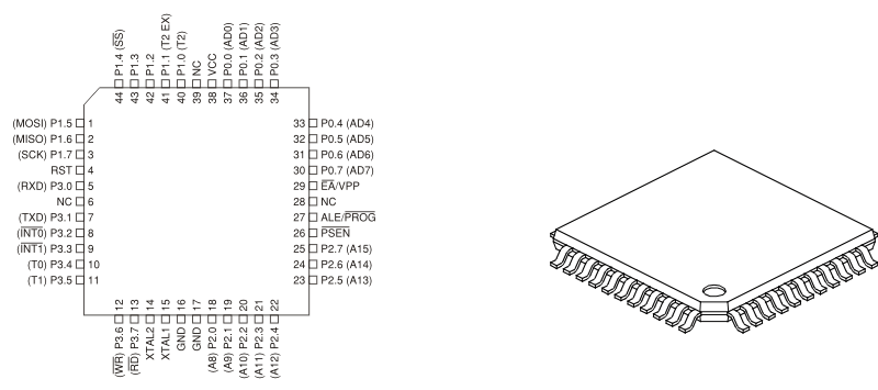
The P89C51 comes in the following packages:

4.2 Pinout Description
VCC Power supply voltage (4-6V)
GND Ground ( Negative supply pole)
Port 0 (P0.0-P0.7) If configured as outputs, each of these pins can be connected to up to 8 TTL inputs. If configured as inputs, the pins can be used as high-impedance inputs as their potential is not defined relative to ground, i.e. they are floating. If additional (external) memory is used, these pins are used for accessing it. Signal on the ALE pin determines what and when will be transferred to this port.
Port 1 (P1.0-P1.7) If configured as outputs, each of these pins can be connected to up to 4 TTL inputs. When configured as inputs, these pins act as standard TTL inputs, that is, each of them is internally connected to the positive supply voltage via a resistor of relatively high impedance. Power supply voltage provided on these inputs is 5V. Also, the Port 1 pins have alternate functions as shown in the table below:
4.3 The AT89S8253 Microcontroller Memory Organisation
Program Memory (ROM)
Program memory (ROM) with a capacity of 12Kb is designed in FLASH technology, which enables programs to be loaded and erased a large number of times. It is programmed via embedded SPI module (Serial Peripheral Interface). If necessary, it is possible to add external ROM memory chip, although 12Kb of ROM is usually more than enough.
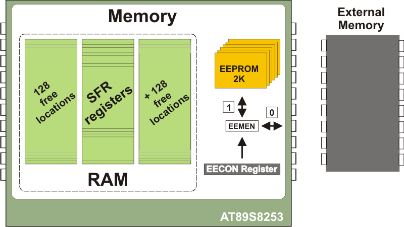
Random Access Memory (RAM)RAM memory consists of 3 blocks containing 128 registers each. Its structure falls into the 8051 standard:
- 128 general-purpose registers;
- 128 memory locations reserved for SFRs. Even though only some of them are trully used, free locations shouldn’t be used for storing variables; and
- 128 additional registers available for use (have no special purpose). Since they have the same addresses as SFRs, they are accessed by indirect addressing.
EEPROM Memory
EEPROM is a special type of memory having features of both RAM and ROM. The contents of the EEPROM may be changed during operation, but remains permanently saved even after the loss of power. The AT89S8253 microcontroller has in total of 2K of EEPROM, that is 2048 locations.
Memory ExpansionAll mentioned above about ROM and RAM memory expansion remains in force when it comes to the AT89S8253 microcontroller as it is based on the 8051 core. In other words, both memories can be added as external chips with the capacity of up to 64Kb. The process of addressing is also the same as in the 8051 standard.
Types of addressingSimilar to all microcontrollers compatible with the 8051, there are two ways of addressing:
- Direct addressing (for example: MOV A,30h); and
- Indirect addressing (for example: MOV A,@R0).
4.4 Special Function Registers (SFRs)
The AT89S8253 microcontroller has in total of 40 Special Function Registers. For the sake of the compatibility with the previous 8051 models, the core registers (22 in total) are the same for all of them, while the others were added later for the purpose of controlling upgraded functions of the microcontroller.
As shown in the table above, each of these registers has its name and specific address in RAM. Unoccupied locations are intended for the future upgraded versions of the microcontroller and shouldn’t be used. As their name suggests, these registers are mostly in control of one specific circuit within the microcontroller such as timers or SPI etc. and they will be discussed later in the book. This chapter covers only those SFRs controlling more than one circuit within the microcontroller.
The accumulator, otherwise marked as ACC or A, belongs to the core registers of the 8051 microcontroller. Its contents is not modified.

B register
The B register also belongs to the core registers of the 8051 microcontroller. Bits of this register are not modified. It is used during multiply and divide operations (MUL and DIV instructions) to store the operands upon which these operations are performed.

PSW register (Program Status Word Register)
The PSW register belongs to the core registers of the 8051 microcontroller. Bits of this register are not modified.

SP registar (Stack Pointer Register)
The SP register belongs to the core registers of the 8051 microcontroller. Bits of this register are not modified.

Registers P0, P1, P2, P3
Each bit of these registers corresponds to one of the port pins having the same name. These registers are therefore used for comminication with peripheral environment which is carried out by sending data from registers to the corresponding pins and vice versa. They belong to the core registers of the 8051 microcontroller and their bits are not modified.
R registers (R0 - R7)
They belong to the core registers of the 8051 microcontroller. Their bits are not modified.
The AUXR register contains only two active bits:
- DISALE
- 0 - ALE is activated at a constant rate of 1/6 the oscillator frequency.
- 1 - ALE is active only during execution of MOVX or MOVC instructions.
- Intel_Pwd_Exit
- 0 - When the microcontroller is in Power Down mode, the program proceeds with execution on high-to-low transition (1-0).
- 1 - When the microcontroller is in Power Down mode, the program proceeds with execution on low-to-high transition (0-1).

CLKREG register (Clock Register) X2

- 0 - The oscillator frequency (the XTAL1 pin) is divided by 2 before used as a clock (machine cycle lasts for 6 such periods).
- 1 - Quartz oscillator is used as a clock generator. This enables the quartz crystal of two times lower frequency (for example 6MHz instead of 12MHz) to be used for the same operating rate of the microcontroller.
Data Pointers
Data Pointers are not true registers as they don’t physically exist. They consist of two separate registers: DPH (Data Pointer High) and DPL (Data Pointer Low). All 16 bits are used for addressing external and internal EEPROM memory. The DPS bit of the EECON register determines the registers to be used as data pointers:
DPS=0 -> Data pointer consists of DP0L and DP0H registers and is marked as DPTR0.
DPS=1 -> Data pointer consists of DP1L and DP1H registers and is marked as DPTR1.

Handling EEPROM memory
2 Kb of on-chip EEPROM memory enables this microcontroller to store data created during operation which must be permanently saved. In other words, all data stored in this memory remains permanently saved even after the loss of power. Minimum 100 000 writing cycles can be executed. This memory is easily used since there are only a few control bits enabling it.
EEPROM write and read is under control of the EECON special function register. Since the process of programming EEPROM is relatively slow (write to one register takes approximately 4mS), a small hardware trick is done in order to speed it up. When the EELD bit of the EECON register is set, the data is not directly written to the EEPROM registers, but loaded in a small buffer (temporary memory) with a capacity of 32 bytes. When this bit is cleared, the first data following it will be normally written to the EEPROM (takes 4 mS) along with all registers currently loaded in the buffer. Thus, it takes only 4mS to write all 32 bytes instead of 128mS otherwise required in a single byte writing.
EEPROM memory is handled in the same way as external memory. For this reason, a special instruction for additional memory chip (MOVX) is also used for EEPROM write and read. The EEMEN bit of the EECON register determines whether the data is to be written/read from additional memory chip or on-chip EEPROM memory.
EECON register
Bits of the EECON register controls the operation of EEPROM memory:

WRTINH
The WRTINH bit is read-only. When the power supply voltage is too low for programming EEPROM, hardware automatically clears this bit, which means that write to EEPROM cannot be completed or is aborted if in progress.
RDY/BSYThe RDY/BSY bit is read-only.
- 0 - Write in progress (takes approximately 4mS).
- 1 - Write complete (data is written to EEPROM).
- 0 - Address for EEPROM write/read is stored in the DP0H and DP0L registers.
- 1 - Address for EEPROM write/read is stored in the DP1H and DP1L registers.
- 0 - Instruction MOVX is used for accessing external memory chip.
- 1 - Instruction MOVX is used for accessing internal EEPROM memory. If the register address is larger than 2K, the microcontroller will access external memory chip.
When set, the EEMWE bit enables write to EEPROM using the MOVX instruction. After completing EEPROM write, the bit must be cleared from within the program.
EELDWhen set, the EELD bit enables up to 32 bytes to be written simultaneously. The bit is set and the MOVX instruction writes data to EEPROM (buffer is loaded). The bit is cleared before writing the last data. When the last MOVX is executed, the entire buffer is automatically loaded to EEPROM for 4mS.
4.5 Watchdog Timer (WDT)
The watchdog timer uses pulses generated by the quartz oscillator for its operation. It is disabled after reset and during Power Down Mode, thus having no effect on the program execution. If enabled, every time it counts up to the program end, the microcontroller reset occurs and program execution starts from the first instruction. Reset condition indicates that the program doesn’t work properly for some reason. The point is to prevent this from happening by setting instruction to reset the watchdog timer at the appropriate program location. Practically, the whole this process is in control of several bits of the WDTCON register.
Three bits (PS2, PS1 and PS0), which are in control of the prescaler, determine the most important feature of the watchdog timer- nominal time, i.e. time required to count up a full cycle.
The values contained in the table below are applied only when the 12MHz quartz oscillator is used.
| Prescaler Bits | Nominal Time | ||
| PS2 | PS1 | PS0 | |
| 0 | 0 | 0 | 16ms |
| 0 | 0 | 1 | 32ms |
| 0 | 1 | 0 | 64ms |
| 0 | 1 | 1 | 128ms |
| 1 | 0 | 0 | 256ms |
| 1 | 0 | 1 | 512ms |
| 1 | 1 | 0 | 1024ms |
| 1 | 1 | 1 | 2048ms |
WDTCON Register (Watchdog Control Register)

PS2,PS1,PS0
These three bits are in control of the prescaler and determine the nominal time of the watchdog timer. If the program doesn’t clear the WSWRST bit during that time, the watchdog timer will reset the microcontroller. When all three bits are cleared to 0, the watchdog timer has a nominal period of 16K machine cycles. When all three bits are set to 1, the nominal period is 2048K machine cycles.
WDIDLE
The WDIDLE bit enables/disables the watchdog timer in Idle mode:
- 0 - Watchdog timer is enabled in Idle mode (low-consumption mode).
- 1 - Watchdog timer is disabled in Idle mode.
DISRTO
The DISRTO bit enables/disables reset of peripheral circuits connected to the RST pin:
- 0 - Watchdog controls the state of the input reset pin. At the moment of reset, this pin acts for a moment as an output and generates a logic one (1). It causes the microcontroller and all other circuits connected to the RST pin to be reset.
- 1 - Reset triggered by the watchdog timer doesn’t affect the state of the reset pin. At the moment the watchdog timer resets the microcontroller, the reset pin remains configured as an input.
HWDT
The HWDT bit selects hardware or software mode for the watchdog timer:
- 0 - Watchdog is in software mode and can be enabled or disabled by the WDTEN bit.
- 1 - Watchdog is in hardware mode. To enable it, the sequence 1E/E1(hex) should be written to the WDTRST register. Only reset condition can disable the watchdog timer. In order to prevent the WCDT from resetting the microcontroller when the nominal time expires, the same sequence 1E/E1hex must be constantly repeated.
WSWRST
When set, this bit resets the watchdog timer in software mode (bit HWDT=0). In order to enable the microcontroller to operate without being interrupted, this bit must regularly be cleared from within the program. After being set, the watchdog timer is cleared by hardware, counting starts from zero and the bit is automatically cleared.
If the watchdog timer is in hardware mode, setting this bit has no effect on the watchdog timer operation.
WDTEN
The WDTEN bit enables/disables the watchdog timer in software mode (HWDT=0):
- 0 - Watchdog disabled.
- 1 - Watchdog enabled.
When the watchdog timer is in hardware mode (HWDT=1), this bit is read-only and reflects the status of the watchdog timer (whether it is enabled or disabled).
![]() The WDTEN bit doesn’t clear the watchdog timer, it only enables/disables it. This means that the current state of the counter remains unchanged as long as WDTEN=0.
The WDTEN bit doesn’t clear the watchdog timer, it only enables/disables it. This means that the current state of the counter remains unchanged as long as WDTEN=0.
4.6 Interrupts
The AT89S8253 has in total of six interrupt sources, which means that it can recognize up to 6 different events that can interrupt regular program execution. Each of these interrupts can be individually enabled or disabled by setting bits of the IE register, whereas the whole interrupt system can be disabled by clearing the EA bit of the same register.
Since this microcontroller has embedded Timer T2 and SPI (they don't fall under the “8051 Standard”) which can generate an interrupt, it was necessary to make some changes in registers controlling interrupt system. Besides, there is a new interrupt vector (address 2B), i.e. program memory address from which the program proceeds with execution when the Timer T2 generates an interrupt. All these changes are made on the previously unused bits. This enables all programs written for the previous versions of the microcontrollers to be used in this one too without being modified. This is why the 8051-based microcontrollers are so popular.
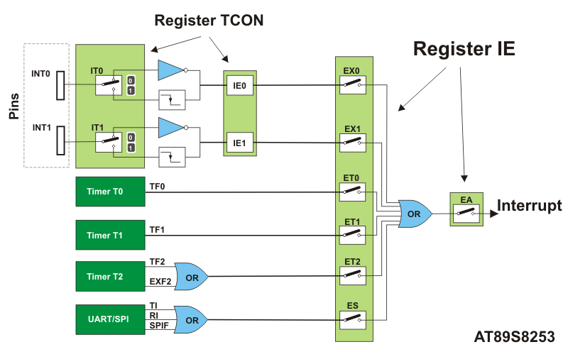
IE register (Interrupt Enable Register)

EA bit enables or disables all interrupt sources (globally):
- 0 - disables all interrupts (even enabled).
- 1 - enables specific interrupts.
ET2 bit enables or disables Timer T2 interrupt:
- 0 - Timer T2 interrupt disabled.
- 1 - Timera T2 interrupt enabled.
ES bit enables or disables serial communication (UART and SPI) interrupts:
- 0 - UART and SPI interrupt disabled.
- 1 - UART and SPI interrupts enabled.
ET1 bit enables or disables Timer T1 interrupt:
- 0 - Timer T1 interrupt disabled.
- 1 - Timer T1 interrupt enabled.
EX1 bit enables or disables external interrupt through the INT0 pin:
- 0 - Interrupt on the INT0 pin disabled.
- 1 - Interrupt on the INT0 pin enabled.
ET0 bit enables or disables Timer T0 interrupt:
- 0 - Timer T0 interrupt disabled.
- 1 - Timer T0 interrupt enabled.
EX0 bit enables or disables external interrupt through the INT1 pin:
- 0 - Interrupt on the INT1 pin disabled.
- 1 - Interrupt on the INT1 pin enabled.
When several interrupts are enabled, it may happen that while one of them is in progress, another one is requested. In such situations, the microcontroller needs to know whether to proceed with the execution of current interrupt routine or to meet a new interrupt request. For this reason, there is a priority list on the basis of which the microcontroller knows what to do. The previous versions of the microcontrollers differentiate between two priority levels defined in the IP register.
As for the AT89S8253 microcontroller, there is an additional SFR register IPH which enables all the interrupts to be assigned 1 out of 4 priorities (excluding reset). Here is a list of priorities:
- Reset. If a reset request arrives, all processes are stopped and the microcontroller restarts.
- The high priority interrupt (3) can be disabled by reset only.
- The low priority interrupt (2, 1 or 0) can be disabled by any high priority interrupt and reset.
It is usually defined at the beginning of the program which one of the existing interrupt sources have high and which one has low priority level. According to this, the following occurs:
- If two interrupt requests, at different priority levels, arrive at the same time then the higher priority interrupt is always serviced first.
- If the both interrupt requests, at the same priority level, occur one after another, the one which came later has to wait until routine being in progress ends.
- If two interrupt requests of equal priority arrive at the same time then the interrupt to be serviced is selected according to the following priority list :
- External interrupt INT0
- Timer T0 interrupt
- External interrupt INT1
- Timer T1 interrupt
- Serial communication interrupt
- Timer T2 Interrupt
IP register (Interrupt Priority Register)

Bits of this register determine the interrupt source priority.
PT2 Timer T2 interrupt priority:
- 0 - Priority 0
- 1 - Priority 1
PS Serial port interrupt priority:
- 0 - Priority 0
- 1 - Priority 1
PT1 Timer T1 interrupt priority:
- 0 - Priority 0
- 1 - Priority 1
PX1 External interrupt INT1 priority:
- 0 - Priority 0
- 1 - Priority 1
PT0 Timer T0 interrupt priority:
- 0 - Priority 0
- 1 - Priority 1
PX0 External interrupt INT0 priority:
- 0 - Priority 0
- 1 - Priority 1
IPH Register (Interrupt Priority High)

PT2H Timer T2 interrupt priority
PSH Serial port interrupt priority
PT1H Timer T1interrupt priority
PX1H External interrupt INT1 priority
PT0H Timer T0 interrupt priority
PX0H External interrupt INT0 Priority
Bits of this register can be combined with appropriate bits of the IP register. This is how a new priority list with 4 interrupt priority levels (5 including reset) is obtained.
| IP bit | IPH bit | Interrupts |
| 0 | 0 | Priority 0 (lowest) |
| 0 | 1 | Priority 1 (low) |
| 1 | 0 | Priority 2 (high) |
| 1 | 1 | Priority 3 (highest) |
When an interrupt request arrives, the microcontroller automatically detects the interrupt source and the following occurs:
- Instruction in progress is ended;
- The address of the next instruction to execute is pushed onto the stack;
- Depending on which interrupt is requested, one of five vectors (addresses) is written to the program counter according to the table below:
| Interrupt Source | Jump Address |
| IE0 | 3h |
| TF0 | Bh |
| IE1 | 13h |
| TF1 | 1Bh |
| RI, TI, SPIF | 23h |
| TF2, EXF2 | 2Bh |
| All addresses are in hex format | |
Appropriate subroutines processing interrupts are stored at these addresses. Instead of them, there are usually jump instructions specifying locations at which these subroutines reside.
4. When an interrupt routine is executed, the address of the next instruction to be executed is popped from the stack to the program counter and the program proceeds from where it left off.
4.7 Counters and Timers
Timers T0 and T1
The AT89S8253 has three timers/counters marked as T0, T1 and T2. Timers T0 and T1 completely fall under the 8051 Standard. There are no changes in their operation.
Timer T2
Timer 2 is a 16-bit timer/counter installed only in new versions of the 8051 family. Unlike timers T0 and T1, this timer consists of 4 registers. Two of them, TH2 and TL2, are connected serially in order to form a larger 16-bit timer register. Like timers 0 and 1, it can operate either as a timer or as an event counter. Another two registers, RCAP2H and RCAP2L, are also serially connected and operate as capture registers. They are used to temporarily store the contents of the counter register.
The main adventage of this timer compared to timers 0 and 1 is that all read and swap operations are easily performed using one instruction. Similar to T0 and T1, it has four different modes of operation to be described later in this chapter.

T2CON (Timer/Counter 2 Control Register)

This register contains bits controlling the operation of timer 2.
TF2 bit is automatically set on timer 2 overflow. In order to detect the next overflow, this bit must be cleared from within the program. If bits RCLK and TCLK are set, overflow has no effect on the TF2 bit.
EXF2 bit is automatically set when a capture or a reload is caused by a negative transition on the T2EX pin. It generates an interrupt (if enabled), unless the DCEN bit of the T2CON register is set. The EXF2 bit must be cleared from within the program.
RCLK is receive clock bit which determines which timer is to be used as receive clock for serial port:
* 1 - T2 is used as receive clock for serial port.
* 0 - T1 is used as receive clock for serial port.
TCLK is transmit clock bit which determines which timer is to be used as transmit clock for serial port:
* 1 - T2 is used as transmit clock for serial port.
* 0 - T1 is used as transmit clock for serial port.
EXEN2 is timer 2 external enable bit used to include the T2EX pin in timer 2 operation:
* 1 - Signal on the T2EX pin affects timer 2 operation.
* 0 - Signal on the T2EX pin is ignored.
TR2 is timer 2 run control bit used to enable/disable timer 2:
* 1 - Timer 2 enabled.
* 0 - Timer 2 disabled.
C/T2 is timer/counter 2 select bit used to select pulses to be counted by counter/timer 2:
* 1 - 16-bit register (T2H and T2L) counts pulses on the C/T2 pin (counter).
* 0 - 16-bit register (T2H and T2L) counts pulses from the oscillator (timer).
CP/RL2 is timer 2 capture/reload bit used to define transfer direction:
* 1 - If EXEN=1, pulse on the T2EX pin will cause a number to be transferred from counter to capture register.
* 0 - Under the same condition, signal on the T2EX pin will cause a number to be transferred from capture to counter register.
Timer T2 in Capture mode
If the CP/RL2 bit of the T2CON register is set, timer 2 operates according to the figure below. This is so called Capture mode in which the value of the counter register (consisting of RCAP2H and RCAP2L) can be “captured” and copied to the capture register (consisting of RCAP2H and RCAP2L), thus not affecting the counting process. This is how it operates:
First, it is necessary to write a number from which the counting starts to a 16-bit register (TH2+TL2).
Timer 2 is enabled by setting the TR2 bit of the TCON register. Each coming pulse increments the number stored in the 16-bit register by 1. When both registers are loaded (decimal number 65536), the first next pulse causes an overflow, reset occurs and counting starts from zero.
Settings:
Timer T2 in auto-reload mode
The auto-reload mode configures timer 2 as a 16-bit timer or event counter with automatic reload. It is controlled by the DCEN bit of the T2MOD register. Setting the DCEN bit enables timer 2 to count up or down from the specified value. The T2EX pin controls the counting direction:
T2OE - Enables timer 2 to operate as independent clock generator.
DCEN - When set, it enables counting in either direction- "up" and "down".
As seen in figure above, unlike Capture mode, the contents of the capture register (RCAP2H, RCAP2L) is now copied in the opposite direction upon an overflow occurs, from capture (RCAP2H, RCAP2L) to counter register (TH2, TL2).
Settings of Auto Reload mode are shown in the table below:
All previously mentioned about timer 2 is in force only if the T2MOD register hasn't been changed, i.e. if DCEN = 0. Otherwise, timer/counter is enabled to count in either direction, which depends on the T2EX pin:
T2EX = 0 Timer 2 counts down
T2EX = 1 Timer 2 counts up
On counting up, the whole procedure is similar to the previous mode with one exception referring to the function of the EXF2 bit.
On counting down, an overflow occurs when values stored in the counter and capture registers match. It causes the TF2 bit as well as all bits of registers T2H and T2L to be set while the counter keeps on counting down: 65535, 65534,65533...
In either case, the EXF2 bit is assigned a new function. When an overflow occurs, this bit inverts the signal and cannot be used for generating an interrupt anymore. Instead, it serves as supplementary bit (the 17th bit) of the counter register, making this counter virtually a 17-bit register.
Timer T2 as a baud rate generatorThe Timer T2 can be used as a baud rate generator and a clock generator simultaneously. If the RCLK or TCLK bit of the register TCON is set, timer T2 turns into a clock generator, so called Baud Rate generator). This mode is very similar to auto-reload mode. The baud rate is computed using the following formula:
There are a few details to be aware of:
- This formula works only if the internal oscillator is used as a clock generator (in this mode, clock is divided by 2, instead of 12)
- Overflow has no effect on the TF2 bit and does not generate an interrupt.
- Whether the EXEN2 bit is set or not, the T2EX pin logic state has no effect on the timer. It means that the T2EX pin can be used as an external interrupt source in this mode.
- Timer should be disabled (TR2=0) prior to writing or reading from registers TH2 and TL2. Otherwise, an error in serial communication might occur.
As previously mentioned, timer T2 can also be used as a clock generator. In all previous examples, the P1.0 pin (marked as T2 in figures) is used as an alternative clock generator for this timer, i.e. it acts as an input. Besides, it can also output pulses. By using a 16MHz quartz crystal, the frequency of pulses it generates ranges from 61Hz to 4MHz with a 50% duty-cycle.
To configure this pin as an output, the C/T2 bit of the T2CON register must be cleared, whereas the T2OE bit of the T2MOD register must be set. The TR2 bit enables the timer and the pin outputs rectangular waves the frequency of which ca be calculated using the formula below:
4.8 Universal Asynchronous Receiver Transmitter (UART)
The Universal Asynchronous Receiver Transmitter (UART) has the same features as that of the standard 8051 microcontrollers. It means that it can operate in 1 out of 4 different modes, which is controlled by bits SM0 and SM1 of the SCON register.
Multiprocessor Communication
Multiprocessor communication (the SM2 bit of the SCON register is set) enables automatic address recognition by allowing the serial port to examine the adress of each incoming command. The process of writing a program is much easier therefore as the microcontrollers sharing the same interface don't have to check each address received via the serial port. Let's make it clear.
Two special function registers, SADDR and SADEN, enable multiprocessor communication. Each device has an individual address that is specified in the SADDR register, while the so called mask address is written to the SADEN register. The mask address contains don't care bits which provide the flexibility to address one or more slaves at a time. In other words, it defines which bits of the SADDR register are to be used and which are to be ignored.
When the master wants to transmit data to one of several slaves, it first sends out an address byte which identifies the target device. An address byte differs from a data byte in that the 9th bit is 1 in an address byte and 0 in a data byte. After receiving the address byte, all slaves check whether it matches their address. The adressed slave clears its SM2 bit and prepares to receive the data bytes to come. The slaves that weren't addressed leave their SM2 bits set and ignores the coming data bytes.
The most simple example is a “mini-network” comprising only 3 microcontrollers:
Microcontroller A is the master and communicates with devices “B” and “C”
Although both microcontrollers B and C are assigned the same address (1100 0000), the mask in register SADEN is used to differentiate between them. It enables the master to communicate with both of them separately or at the same time:
If transmit address is 1100 0010, the data will be sent to slave device B.
If transmit address is 1100 0001 the data will be sent to slave device C.
If transmit address is 1100 0000 the data will be sent to both slave devices.
4.9 SPI System (Serial Peripheral Interface)
In addition to UART system, the AT89S8253 has also another system for serial communication which doesn’t fall into the 8051 Standard. It is SPI system which provides a high-speed synchronous data transfer between the microcontroller and one or more peripheral devices or between multiple microcontrollers. Here, one microcontroller is always considered main and is called master therefore. It defines rate, transfer direction (whether data is to be transferred or received) and data format. The other is slave device which is in subordinated position, which further means that it cannot start data transfer, but has to adjust to conditions set by the master device.
The data are transferred via full duplex connection using 3 conductors connected to pins MISO (P1.6), MOSI (P1.5) and SCK (P1.7). The forth pin-control pin SS- is not used on the master side and may be used as a general-purpose input/output therefore, while on the slave side it must have voltage level 0. When the SS pin on the slave side is set, its SPI system is deactivated and the MOSI pin can be used as a general-purpose input.
As shown on the schematic, pins MISO and MOSI are configured differently in the master and slave device (as inputs or outputs), which is determined by the MSTR bit of the SPCR register.
![]() Knowing abbraviations makes connection easier:
Knowing abbraviations makes connection easier:
MISO - master in, slave out; MOSI - master out, slave in; SCK - serial clock; SS - slave select;
Similar to many other circuits within the microcontroller, the SPI system can also be configured to operate in several modes.
Normal SPI mode (buffer out of use)Data written to the SPI data register SPDR is automatically transferred to an 8- bit shift register. SPI clock generator is enabled and serial data appears on the MOSI pin. An initial delay may occur for the sake of synchronization with the main oscillator.
After sending one byte, the SPI clock generator stops, the SPIF bit (flag) is set, the received byte is transferred to the SPDR register and, if enabled, an interrupt is generated.
Any attempt to write another byte to the SPDR register while byte transmit is in progress will cause the WCOL bit to be set. It indicates that an error has occured. However, the byte will be succesfully transmitted, while the new byte will be ignored, i.e. it will not be transmitted.
Enhanced SPI mode (buffer in use)Enhanced mode is similar to normal except that this time data goes through one more register while being transmitted. It makes no sense at first sight, but communication is really faster. Look at the figure below...
Data written to the SPI data register SPDR is automatically transferred to the capture register (buffer), which causes the WCOL bit to be set. It means that the buffer is full and any further write will cause an overflow. Control electronics (hardware) cleares this bit after transmitting data from buffer to the shift register and after commencing serial data transmit. If the byte sent is the first, the data is immediately transmitted to the shift register (still empty), thus clearing the WCOL bit (buffer is empty).
While one byte transmit is in progress, the next byte to transmit may be written to the SPDR register. It will be immediately moved to buffer. In order to check whether data transmit is in progress, it is sufficient to check the logic state of the LDEN bit of the SPSR register. If this bit is set (Load Enable) and the WCOL bit is cleared, data transmit is in progress and buffer is empty so the next byte can be written to the SPDR register.
How to select the right mode? If individual bytes are sent occasionally then there is no need to complicate- the best solution is the normal mode. If it is necessary to send a great amounts of data, it is better to use enhanced mode in which the clock oscillator is enabled as far as buffer is regularly loaded and the WCOL bit is set. In addition, no time is needed for synchronization and data is easily and efficiently transferred.
The SPI system is under control of 3 special function registers. These are SPDR, SPSR and SPCR.
SPDR (SPI Data Register)The SPDR register is used for storing data to be transferred via SPI (in serial format). It is also used for storing received data.
SPIF Interrupt flag. Upon data transfer, this bit is automatically set and an interrupt is generated if SPIE=1 and ES=1. The SPIF bit is cleared by reading SPSR followed by reading/writing SPDR register.
WCOL This bit is set in normal mode (ENH=0) if the SPDR register is written during data transfer is in progress. The write is premature and has no effect. It is called Write Collision. This bit is cleared in the same manner as the SPIF bit.
The bit is set in enhanced mode (ENH=1) when buffer is full. It is indication that a new data is ready to be transmitted to the shift register.
In enhanced mode, a new data can be written to buffer when the WCOL bit is set. In addition, the WCOL bit must be cleared.
DISSO When set, this bit causes the MISO pin to float, thus enabling several slave microcontrollers to share the same interface. Normally, the first byte, called address byte, is received by all of them, but only one should clear its DISSO bit.
ENH
0 SPI system operates in normal mode (without buffer).
1 SPI system operates in enhanced mode.
SPIE When this bit is set, the SPI system can generate an interrupt.
SPE This bit enables SPI communication. When set, pins SS, MOSI, MISO and SCK are connected to the microcontroller pins P1.4, P1.5, P1.6 and P1.7.
DORD Bit determines which bytes in serial communication are to be sent first:
- 0 - MSB bit is sent first.
- 1 - LSB bit is sent first.
MSTR Bit determines whether the microcontroller is to operate as master or slave:
- 0 - Operate as slave.
- 1 - Operate as master.
CPOL Bit controls the SCK pin logic state when the SPI communication is not in progress:
- 0 - Pin SCK is cleared.
- 1 - Pin SCK is set.
CPHA This bit along with the CPOL bit controls relation between clock and data in serial format. Refer to the figure below.
SPR1,SPR0 When SPI system operates as master, these two bits determine boud rate, i.e. clock signal frequency of the master device. When operates as slave, these bits have no effect and SPI system operates at a rate imposed by the master device.
| SPR1 | SPR0 | SCK |
| 0 | 0 | Fosc/4 |
| 0 | 1 | Fosc/16 |
| 1 | 0 | Fosc/64 |
| 1 | 1 | Fosc/128 |
Serial data format if CPHA=0
* not defined. It is usually MSB of previously received byte.
Serial data format if CPHA=1
* not defined. It is usually LSB of previously received byte.
![]()
Two things are important to remember when configuring SPI system:
- Master should be configured before slave.
- When writing bits to the SPCR register, the SPE bit enabling SPI should be set last, i.e. after setting all other parameters.
4.10 Power Consumption Control
Like all models belonging to the 8051 series, this microcontroller can operate in 1 out of 3 modes: normal (consumption ca. 25 mA), Idle (consumption ca. 6.5 mA) and Power Down (consumption ca. 40 uA). The mode of operation is selected by bits of the PCON register (Power Control Register). Three bits are changed compared to the basic model:
The purpose of the bits of the PCON register:
SMOD1 When set, this bit makes boud rate twice as high.
SMOD0 Bit determines the purpose of the 7th bit of the SCON register:
- 0 Seventh bit of the SCON register has the function of SM0, i.e. selects mode of operation.
- 1 Seventh bit has the function of FE, i.e. detects errors. It is rarely used.
POF Bit is automatically set when the voltage level reaches maximum (must be higher than 3V) after powering on. It is used for detecting cause for reset (power on or restart condition after exiting Power Down mode).
GF1 General purpose bit (available for use).
GF0 General purpose bit (available for use).
PD By setting this bit, the microcontroller is set in Power Down mode.
IDL By setting this bit, the microcontroller is set in Idle mode. When something goes wrong...
If something unexpected happens during the operation of the microcontroller, what most bothers is the fact that it’s never the microcontroller's fault. Although it’s not self-evident, the microcontroller always obediently follows program instructions. For this reason, it is necessary to pay special attention to several “critical points” when writing a program. The first one is RAM memory.
Even though it is designed to meet needs of the majority of users and has all required, a memory space intended for RAM is still only a single entity. It means that there are no phisically separated registers R0-R7, general purpose registers, stack etc. Instead, these are differently designated parts of the same “memory shelf”. Refer to the figure below.
If we neglect this “detail”, there is a risk that the program suddenly starts to perform unpredictably. In order to prevent it, it is necessary to take care of the following:
If only registers R0-R7 from bank 0 are in use, everything is easily kept under control and program memory locations from 08h to 1Fh are available for use. If registers, otherwise having the same names, from some other bank are in use, you should be careful when using locations whose addresses are less than 20h because it can cause “R” registers to be erased.
If bit-variables are not used in the program, program memory locations 20h-2Fh are available for use. If the program contains bit-variables, you should be careful when using these location in order not to change them accidentaly.
By default, the data pushed onto stack occupy program memory locations starting from 08h. If the banks 1, 2 or 3 are in use, their contents will be certainly erased. For this reason, it is recommended to set the Stack Pointer value to be greater than 20h or even greater at the beginning of the program.
SFRs are used for controlling the microcontroller operation. Each of them has its specific purpose and it should be observed. It means that they cannot be used as general purpose registers even in the event that some of their locations is not occupied.
Instruction set, recognized by the microcontroller, contains instructions which can be used for controlling individual bits of registers at program memory location 20h-7Fh. Besides, individual bits of some SFRs (not all of them) can also be directly accessed. Addresses of these registers are divisible by 8.
If memory is expanded by adding external RAM or ROM memory chip, ports P0 and P2 are not available for use regardless of how many pins are actually used for memory expansion.
The DPTR register is a 16-bit register comprised of registers DPH and DPL which are 8-bit wide each. The DPTR register should be considered like that practically. For example, when pushing it onto the Stack, DPL should be pushed first, then DPH.
When used, serial communication is under control of the SCON register. Besides, registers TCON and TMOD should be configured for this purpose as well since the timer T1 is mostly used for boud rate generation.
When some of the interrupts is enabled, you should be careful because there is a risk that program starts to perform unexpectedly. When an interrupt request arrives, the microcontroller will execute instruction in progress, push the address of the first following location onto the stack (in order to know from where to continue) and jump to the specified interrupt routine address. When the routine has been executed, the microcontroller will pop the address from the stack and continue from where it left off. However...
The microcontroller saves only the address to continue from after routine execution. What is usually neglected is the fact that the contents of many registers can be changed during routine execution. The program normally procedees with execution considering the changed registers correct if their original vaules haven't been saved, thus causing a total chaos. The worst thing is that this problem can be manifested anytime: at the moment or several days later (depending on the moment an interrupt occurs). Obviously, the only solution is to save the state of all important registers at the beginning of interrupt routine and to update these values before returning to the program. We are actually talking about the following registers:
- PSW
- DPTR (DPH, DPL)
- ACC
- B
- Registers R0 - R7
![]() Contents of registers are usually saved by being pushed onto the Stack using the PUSH instruction. However, instructions such as “PUSH R0” cannot be used here because the microcontroller “doesn’t know” which register is concerned as there are 4 banks with registers haing the same names R0-R7. For this reason, it is necessary to save addresses of these registers instead of their names using the PUSH 00h instruction.
Contents of registers are usually saved by being pushed onto the Stack using the PUSH instruction. However, instructions such as “PUSH R0” cannot be used here because the microcontroller “doesn’t know” which register is concerned as there are 4 banks with registers haing the same names R0-R7. For this reason, it is necessary to save addresses of these registers instead of their names using the PUSH 00h instruction.
When some of the instructions for indirect addressing is used, you should be careful not to use them for accessing SFRs as the microcontroller ignores their addresses and accesses free RAM locations having the same addresses as SFRs.
When UART system for serial communication is used, setting bits RI and TI of the SCON register generated the same interrupt. If such an interrupt is generated, it is first necessary to detect interrupt source (byte is sent, received or both). It is important to remember that the microcontroller only sets these bits so that they must be cleared from within the program. Otherwise, the program gets stuck and executes the same interrupt routine over and over again.
Chapter 5: Assembly Language
- 5.1 Elements of Assembly Language
Introduction
It was time that hardware-oriented to the core made compromise if they wanted to stay “in the game”. Namely, unlike other circuits which only need to be connected to other components and powered in order to be of any use, microcontrollers require to be programmed as well. Fortunately, they still didn't progress so far in their evolution, so that all microcontroller families “understand” only one language - machine language. That's a good thing. The bad one is that, even primitive, this language of zeros and ones can only be understood by microcontrollers and some of the experts working on its development. In order to bridge this gap between machine and humans, the first high-level programming language called Assembly language was created.
The main problem of remembering codes recognized as instructions by electronics was solved therefore, but another one, equally complicated to both us and “them”(microcontrollers) arose. This problem was also easily solved by means of the program for a PC called assembler and a simple device called programmer.
This program enables the PC to receive commands in the form of abbreviations and convert them unerringly into so called “executable file”. The moment of compiling a program into machine language is crucial as this file, called HEX file, represents a series of binary numbers understandable to microcontrollers only. The program written in assembly language cannot be executed practically unless this file is loaded into the microcontroller memory. This is the moment when the last link in the chain - the programmer - appears on the scene. It is a small device connected to a PC via some of the ports and has a socket for placing chip in.
5.1 Elements of Assembly Language
Assembly language is basically like any other language, which means that it has its words, rules and syntax. The basic elements of assembly language are:
- Labels;
- Orders;
- Directives; and
- Comments.
Syntax of Assembly language
When writing a program in assembly language it is necessary to observe specific rules in order to enable the process of compiling into executable “HEX-code” to run without errors. These compulsory rules are called syntax and there are only several of them:
- Every program line may consist of a maximum of 255 characters;
- Every program line to be compiled, must start with a symbol, label, mnemonics or directive;
- Text following the mark “;” in a program line represents a comment ignored (not compiled) by the assembler; and
- All the elements of one program line (labels, instructions etc.) must be separated by at least one space character. For the sake of better clearness, a push button TAB on a keyboard is commonly used instead of it, so that it is easy to delimit columns with labels, directives etc. in a program.
Numbers
If octal number system, otherwise considered as obsolite, is disregarded, assembly laguage allows numbers to be used in one out of three number systems:
Decimal Numbers
If not stated otherwise, the assembly language considers all the numbers as decimal. All ten digits are used (0,1,2,3,4,5,6,7,8,9). Since at most 2 bytes are used for saving them in the microcontroller, the largest decimal number that can be written in assembly language is 65535. If it is necessary to specify that some of the numbers is in decimal format, then it has to be followed by the letter “D”. For example 1234D.
Hexadecimal Numbers
Hexadecimal numbers are commonly used in programming. There are 16 digits in hexadecimal number system (0, 1, 2, 3, 4, 5, 6, 7, 8, 9, A, B, C, D, E, F). The largest hexadecimal number that can be written in assembly language is FFFF. It corresponds to decimal number 65535. In order to distinguish hexadecimal numbers from decimal, they are followed by the letter “h”(either in upper- or lowercase). For example 54h.
Binary Numbers
Binary numbers are often used when the value of each individual bit of some of the registers is important, since each binary digit represents one bit. There are only two digits in use (0 and 1). The largest binary number written in assembly language is 1111111111111111. In order to distinguish binary numbers from other numbers, they are followed by the letter “b” (either in upper- or lowercase). For example 01100101B.
Operators
Some of the assembly-used commands use logical and mathematical expessions instead of symbols having specific values. For example:
Chapter 6 : Examples
- 6.1 Basic connecting of the microcontroller
- 6.2 Additional components
- 6.3 Examples
Introduction
The purpose of this chapter is to provide basic information about microcontrollers that one needs to know in order to be able to use them successfully in practice. This is why this chapter doesn't contain any super interesting program or device schematic with amazing solutions. Instead, the following examples are better proof that program writing is neither a privilege nor a talent issue, but the ability of simply putting puzzle pieces together using directives. Rest assured that design and development of devices mainly consists of the following method “test-correct-repeat”. Of course, the more you are in it, the more complicated it becomes since the puzzle pieces are put together by both children and first-class architects...
6.1 Basic connecting

As seen in the figure above, in order to enable the microcontroller to operate properly it is necessary to provide:
- Power supply:
- Reset signal: and
- Clock signal.
Clearly, it is about very simple circuits, but it does not have to be always like that. If the target device is used for controlling expensive machines or maintaining vital functions, everything gets increasingly complicated. However, this solution is sufficient for the time being...
Power supply
Even though this microcontroller can operate at different power supply voltages, why to test “Murphy’s low”?! A 5V DC is most commonly used. The circuit, shown in the figure, uses a cheap integrated three-terminal positive regulator LM7805, and provides high-quality voltage stability and quite enough current to enable the microcontroller and peripheral electronics to operate normally (enough current in this case means 1Amp).
Reset signal
In order that the mucrocontroller can operate properly, a logic 0 (0V) must be applied to the reset pin RS. The push button connecting the reset pin RS to power supply VCC is not necessary. However, it is almost always provided because it enables the microcontroller safe return to normal operating conditions if something goes wrong. 5V is brought to this pin, the microcontroller is reset and program starts execution from the beginning.
Clock signal
Even though the microcontroller has a built-in oscillator, it cannot operate without two external capacitors and quartz crystal which stabilize its operation and determines its frequency (operating speed of the microcontroller).
Of course, it is not always possible to apply this solution so that there are always alternative ones. One of them is to provide clock signal from a special source through invertor. See the figure on the left.
6.2 Additional components
Regardless of the fact that the microcontroller is a product of modern technology, it is of no use without being connected to additional components. Simply put, the appearance of voltage on its pins means nothing if not used for performing certain operations (turn something on/off, shift, display etc.).
Switches and Push buttons
There are no simpler devices than switches and push-buttons. This is the simplest way of detecting appearance of a voltage on the microcontroller input pin.
 Nevertheless, it is not so simple in practice... It is about contact bounce- a common problem with m e c h a n i c a l switches. When the contacts strike together, their momentum and elasticity act together to cause bounce. The result is a rapidly pulsed electrical current instead of a clean transition from zero to full current. It mostly occurs due to vibrations, slight rough spots and dirt between contacts. This effect is usually unnoticeable when using these components in everyday life because the bounce happens too quickly. In other words, the whole this process does not last long (a few micro- or miliseconds), but it is long enough to be registered by the microcontroller. When using only a push-button as a pulse counter, errors occur in almost 100% of cases!
The simplest solution to this problem is to connect a simple RC circuit to suppress quick voltage changes. Since the bounce period is not defined, the values of components are not precisely determined. In most cases, it is recomended to use the values shown in figure below.
If complete stability is needed then radical measures should be taken. The output of the circuit, shown in figure (RS flip-flop), will change its logic state only after detecting the first pulse triggered by contact bounce. This solution is expensive (SPDT switch), but effecient, the problem is definitely solved. Since the capacitor is not used, very short pulses can also be registered in this way.
 In addition to these hardware solutions, there is also a simple software solution. When a program tests the state of an input pin and detects a change, the check should be done one more time after a certain delay. If the change is confirmed, it means that a switch or push button has changed its position.
The advantages of such solution are obvious: it is free of charge, effects of noises are eliminated and it can be applied to the poorer quality contacts as well. Disadvantage is the same as when using RC filter, i.e. pulses shorter than program delay cannot be registered.
Optocoupler
 An optocoupler is a device commonly used to galvanically separate microcontroller’s electronics from any potentially dangerous current or voltage in its surroundings. Optocouplers usually have one, two or four light sources (LED diodes) on their input while on their output, opposite to diodes, there is the same number of elements sensitive to light (phototransistors, photo-thyristors or photo-triacs). The point is that an optocoupler uses a short optical transmission path to transfer a signal between the elements of circuit, while keeping them electrically isolated. This isolation makes sense only if diodes and photo-sensitive elements are separately powered. In this way, the microcontroller and expensive additional electronics are completely protected from high voltage and noises which are the most common cause of destroying, damaging or unstable operation of electronic devices in practice. The most frequently used optocouplers are those with phototransistors on their outputs. When using the optocoupler with internal base-to-pin 6 connection (there are also optocouplers without it), the base can be left unconnected. An optional connection which lessens the effects of noises by eliminating very short pulses is presented by the broken line in the figure.
Relay
 A relays is an electrical switch that opens and closes under control of another electrical circuit. It is therefore connected to ouput pins of the microcontroller and used to turn on/off high-power devices such as motors, transformers, heaters, bulbs, antenna systems etc. These are almost always placed away from the board sensitive components. There are various types of relays but all of them operate in the same way. When a current flows through the coil, the relay is operated by an electromagnet to open or close one or many sets of contacts. Similar to optocouplers, there is no galvanic connection (electrical contact) between input and output circuits. Relays usually demand both higher voltage and current to start operation, but there are also miniature ones which can be activated by a low current directly obtained from a microcontroller pin.
The figure shows the solution specific to the 8051 microcontroller. A darlington transistor is used here to activate relays because of its high current gain. This is not in accordance with “rules”, but is necessary in the event that logic one activation is applied since the output current is then very low (pin acts as an input).
 In order to prevent the appearance of self-induction high voltage, caused by a sudden stop of current flow through the coil, an inverted polarized diode is connected in parallel to the coil. The purpose of this diode is to “cut off” the voltage peak.
Light-emitting diode (LED)
Light-emitting diodes are elements for light signalization in electronics. They are manufactured in different shapes, colors and sizes. For their low price, low power consumption and simple use, they have almost completely pushed aside other light sources, bulbs at first place. They perform similar to common diodes with the difference that they emit light when current flows through them.
 It is important to limit their current, otherwise they will be permanently destroyed. For this reason, a conductor must be connected in parallel to an LED. In order to determine value of this conductor, it is necessary to know diode’s voltage drop in forward direction, which depends on what material a diode is made from and what colour it is. Typical values of the most frequently used diodes are shown in table below. As seen, there are three main types of LEDs. Standard ones get ful brightness at current of 20mA. Low Current diodes get ful brightness at ten times lower current while Super Bright diodes produce more intensive light than Standard ones.
| Color | Type | Typical current Id (mA) | Maximal current If (mA) | Voltage drop Ud (V) |
| Infrared | - | 30 | 50 | 1.4 |
| Red | Standard | 20 | 30 | 1.7 |
| Red | Super Bright | 20 | 30 | 1.85 |
| Red | Low Current | 2 | 30 | 1.7 |
| Orange | - | 10 | 30 | 2.0 |
| Green | Low Current | 2 | 20 | 2.1 |
| Yellow | - | 20 | 30 | 2.1 |
| Blue | - | 20 | 30 | 4.5 |
| White | - | 25 | 35 | 4.4 |

Since the 8051 microcontroller can provide only low output current and since its pins are configured as outputs when voltage provided on them is 0V, direct connecting to LEDs is performed as shown in figure on the right (Low current LED, cathode is connected to the output pin).
LED displays
 Basically, an LED display is nothing more than several LEDs moulded in the same plastic case. There are many types of displays composed of several dozens of built in diodes which can display different symbols.
Most commonly used is a so called 7-segment display. It is composed of 8 LEDs, 7 segments are arranged as a rectangle for symbol displaying and there is an additional segment for decimal point displaying. In order to simplify connecting, anodes and catodes of all diodes are connected to the common pin so that there are common anode displays and common catode displays, respectively. Segments are marked with the latters from A to G, plus dp, as shown in the figure on the left. On connecting, each diode is treated separtely, which means that each must have its own current limiting resistor.
Displays connected to the microcontroller usually occupy a large number of valuable I/O pins, which can be a big problem especially if it is needed to display multy digit numbers. The problem is more than obvious if, for example, it is needed to display two 6-digit numbers (a simple calculation shows that 96 output pins are needed in this case). The solution to this problem is called MULTIPLEXING. This is how an optical illusion based on the same operating principle as a film camera is made. Only one digit is active at a time, but they change their state so quickly making impression that all digits of a number are simultaneously active.

Here is an explanation on the figure above. First a byte representing units is applied on a microcontroller port and a transistor T1 is activated at the same time. After a while, the transistor T1 is turned off, a byte representing tens is applied on a port and a transistor T2 is activated. This process is being cyclically repeated at high speed for all digits and corresponding transistors.
The fact that the microcontroller is just a kind of miniature computer designed to understand only the language of zeros and ones is fully expressed when displaying any digit. Namely, the microcontroller doesn't know what units, tens or hundreds are, nor what ten digits we are used to look like. Therefore, each number to be displayed must be prepared in the following way:
First of all, a multy digit number must be split into units, tens etc. in a particular subroutine. Then each of these digits must be stored in special bytes. Digits get familiar format by performing “masking”. In other words, a binary format of each digit is replaced by a different combination of bits in a simple subroutine. For example, the digit 8 (0000 1000) is replaced by the binary number 0111 111 in order to activate all LEDs displaying digit 8. The only diode remaining inactive in this case is reserved for the decimal point. If a microcontroller port is connected to the display in such a way that bit 0 activates segment “a”, bit 1 activates segment “b”, bit 2 segment “c” etc., then the table below shows the “mask” for each digit.
| Digits to display | Display Segments | |||||||
| dp | a | b | c | d | e | f | g | |
| 0 | 1 | 0 | 0 | 0 | 0 | 0 | 0 | 1 |
| 1 | 1 | 0 | 0 | 1 | 1 | 1 | 1 | 1 |
| 2 | 1 | 0 | 0 | 1 | 0 | 0 | 1 | 0 |
| 3 | 1 | 0 | 0 | 0 | 0 | 1 | 1 | 0 |
| 4 | 1 | 1 | 0 | 0 | 1 | 1 | 0 | 0 |
| 5 | 1 | 0 | 1 | 0 | 0 | 1 | 0 | 0 |
| 6 | 1 | 0 | 1 | 0 | 0 | 0 | 0 | 0 |
| 7 | 1 | 0 | 0 | 0 | 1 | 1 | 1 | 1 |
| 8 | 1 | 0 | 0 | 0 | 0 | 0 | 0 | 0 |
| 9 | 1 | 0 | 0 | 0 | 0 | 1 | 0 | 0 |
In addition to digits from 0 to 9, some letters of alphabet - A, C, E, J, F, U, H, L, b, c, d, o, r, t - can also be displayed by performing appropriate masking. If the event that common chatode displays are used all units in the table should be replaced by zeros and vice versa. Additionally, NPN transistors should be used as drivers as well.
Liquid Crystal Displays (LCD)
 An LCD display is specifically manufactured to be used with microcontrollers, which means that it cannot be activated by standard IC circuits. It is used for displaying different messages on a miniature liquid crysal display.
The model described here is for its low price and great capabilities most frequently used in practice. It is based on the HD44780 microcontroller (Hitachi) and can display messages in two lines with 16 characters each. It displays all the letters of alphabet, Greek letters, punctuation marks, mathematical symbols etc. In addition, it is possible to display symbols made up by the user. Other useful features include automatic message shift (left and right), cursor appearance, LED backlight etc.
LCD Pins
There are pins along one side of a small printed board. These are used for connecting to the microcontroller. There are in total of 14 pins marked with numbers (16 if it has backlight). Their function is described in the table bellow:
| Function | Pin Number | Name | Logic State | Description |
| Ground | 1 | Vss | - | 0V |
| Power supply | 2 | Vdd | - | +5V |
| Contrast | 3 | Vee | - | 0 - Vdd |
| Control of operating | 4 | RS | 0 1 |
D0 – D7 are interpreted as commands D0 – D7 are interpreted as data |
| 5 | R/W | 0 1 |
Write data (from controller to LCD) Read data (from LCD to controller) |
|
| 6 | E | 0 1 From 1 to 0 |
Access to LCD disabled Normal operating Data/commands are transferred to LCD |
|
| Data / commands | 7 | D0 | 0/1 | Bit 0 LSB |
| 8 | D1 | 0/1 | Bit 1 | |
| 9 | D2 | 0/1 | Bit 2 | |
| 10 | D3 | 0/1 | Bit 3 | |
| 11 | D4 | 0/1 | Bit 4 | |
| 12 | D5 | 0/1 | Bit 5 | |
| 13 | D6 | 0/1 | Bit 6 | |
| 14 | D7 | 0/1 | Bit 7 MSB |
LCD screen
An LCD screen consists of two lines each containing 16 characters. Each character consists of 5x8 or 5x11 dot matrix. This book covers the most commonly used display, i.e. the 5x8 character display.
Display contrast depends on the power supply voltage and whether messages are displayed in one or two lines. For this reason, varying voltage 0-Vdd is applied on the pin marked as Vee. Trimmer potentiometer is usually used for that purpose. Some LCD displays have built-in backlight (blue or green LEDs). When used during operation, a current limiting resistor should be serially connected to one of the pins for backlight power supply (similar to LEDs).

![]() If there are no characters displayed or if all of them are dimmed when the display is on, the first thing that should be done is to check the potentiometer for contrast regulation. Is it properly adjusted? The same applies if the mode of operation has been changed (writing in one or two lines).
If there are no characters displayed or if all of them are dimmed when the display is on, the first thing that should be done is to check the potentiometer for contrast regulation. Is it properly adjusted? The same applies if the mode of operation has been changed (writing in one or two lines).
LCD Memory
The LCD display contains three memory blocks:
- DDRAM Display Data RAM;
- CGRAM Character Generator RAM; and
- CGROM Character Generator ROM.
DDRAM Memory
DDRAM memory is used for storing characters to be displayed. The size of this memory is sufficient for storing 80 characters. Some memory locations are directly connected to the characters on display.

It works quite simply: it is sufficient to configure the display so as to increment addresses automatically (shift right) and set the starting address for the message that should be displayed (for example 00 hex).
After that, all characters sent through lines D0-D7 will be displayed in the message format we are used to- from left to right. In this case, displaying starts from the first field of the first line since the address is 00 hex. If more than 16 characters are sent, then all of them will be memorized, but only the first sixteen characters will be visible. In order to display the rest of them, a shift command should be used. Virtually, everything looks as if the LCD display is a “window” which moves left-right over memory locations containing different characters. This is how the effect of message “moving” on the screen is made.
If the cursor is on, it appears at the location which is currently addressed. In other words, when a character appears at the cursor position, it will automatically move to the next addressed location. Since this is a sort of RAM memory, data can be written to and read from it, but its contents is irretrievably lost when the power goes off.
CGROM MemoryCGROM memory contains the default chracter map with all characters that can be displayed on the screen. Each character is assigned to one memory location.

The addresses of CGROM memory locations match the characters of ASCII. If the program being currently executed encounters a command “send character P to port”, then the binary value 0101 0000 appears on the port. This value is the ASCII equivalent to the character P. It is then written to LCD, which results in displaying the symbol from 0101 0000 location of CGROM. In other words, the character “P” is displayed. This applies to all letters of alphabet (capitals and small), but not to numbers.
As seen on the previous “map”, addresses of all digits are pushed forward by 48 relative to their values (digit 0 address is 48, digit 1 address is 49, digit 2 address is 50 etc.). Accordingly, in order to display digits correctly, each of them needs to be added a decimal number 48 prior to be sent to LCD.
![]() From their inception till today, computers can recognize only numbers, but not letters. It means that all data a computer swaps with a peripheral device has a binary format, even though the same is recognized by the man as letters (keyboard is an excellent example). Every character matches the unique combination of zeroes and ones. ASCII is character encoding based on the English alphabet. ASCII code specifies correspondance between standard character symbols and their numerical equivalents.
From their inception till today, computers can recognize only numbers, but not letters. It means that all data a computer swaps with a peripheral device has a binary format, even though the same is recognized by the man as letters (keyboard is an excellent example). Every character matches the unique combination of zeroes and ones. ASCII is character encoding based on the English alphabet. ASCII code specifies correspondance between standard character symbols and their numerical equivalents.
CGRAM memory
Apart from standard characters, the LCD display can also display symbols defined by the user itself. It can be any symbol in the size of 5x8 pixels. RAM memory called CGRAM in the size of 64 bytes enables it.
Memory registers are 8 bits wide, but only 5 lower bits are used. Logic one (1) in every register represents a dimmed dot, while 8 locations grouped together represent one character. It is best illustrated in figure below:

Symbols are usually defined at the beginnig of the program by simply writing zeros and ones to registers of CGRAM memory so that they form desired shapes. In order to display them it is sufficient to specify their address. Pay attention to the first coloumn in the CGROM map of characters. It doesn't contain RAM memory addresses, but symbols being discussed here. In this example, “display 0” means - display “č”, “display 1” means - display “ž” etc.
LCD Basic CommandsAll data transferred to LCD through the outputs D0-D7 will be interpreted as a command or a data, which depends on the pin RS logic state:
RS = 1 - Bits D0-D7 are addresses of the characters to be displayed. LCD processor addresses one character from the character map and displays it. The DDRAM address specifies the location on which the character is to be displayed. This address is defined before the character is transferred or the address of previously transferred character is automatically incremented.
RS = 0 - Bits D0 - D7 are commands which determine the display mode. The commands recognized by the LCD are given in the table below:
| Command | RS | RW | D7 | D6 | D5 | D4 | D3 | D2 | D1 | D0 | Execution Time |
| Clear display | 0 | 0 | 0 | 0 | 0 | 0 | 0 | 0 | 0 | 1 | 1.64mS |
| Cursor home | 0 | 0 | 0 | 0 | 0 | 0 | 0 | 0 | 1 | x | 1.64mS |
| Entry mode set | 0 | 0 | 0 | 0 | 0 | 0 | 0 | 1 | I/D | S | 40uS |
| Display on/off control | 0 | 0 | 0 | 0 | 0 | 0 | 1 | D | U | B | 40uS |
| Cursor/Display Shift | 0 | 0 | 0 | 0 | 0 | 1 | D/C | R/L | x | x | 40uS |
| Function set | 0 | 0 | 0 | 0 | 1 | DL | N | F | x | x | 40uS |
| Set CGRAM address | 0 | 0 | 0 | 1 | CGRAM address | 40uS | |||||
| Set DDRAM address | 0 | 0 | 1 | DDRAM address | 40uS | ||||||
| Read “BUSY” flag (BF) | 0 | 1 | BF | DDRAM address | - | ||||||
| Write to CGRAM or DDRAM | 1 | 0 | D7 | D6 | D5 | D4 | D3 | D2 | D1 | D0 | 40uS |
| Read from CGRAM or DDRAM | 1 | 1 | D7 | D6 | D5 | D4 | D3 | D2 | D1 | D0 | 40uS |
What is the Busy flag?
Compared to the microcontroller, the LCD is an extremely slow component. Because of this, it was necessary to provide a signal which will, upon command execution, indicate that the display is ready to receive a new data. That signal, called the busy flag, can be read from line D7. When the BF bit is cleared (BF=0), the display is ready to receive a new data.
LCD ConnectionDepending on how many lines are used for connecting the LCD to the microcontroller, there are 8-bit and 4-bit LCD modes. The appropriate mode is selected at the beginning of the operation. This process is called “initialization”. 8-bit LCD mode uses outputs D0-D7 to transfer data in the way explained on the previous page. The main purpose of 4-bit LED mode is to save valuable I/O pins of the microcontroller. Only 4 higher bits (D4-D7) are used for communication, while other may be left unconnected. Each data is sent to the LCD in two steps: four higher bits are sent first (normally through the lines D4-D7), then four lower bits. Initialization enables the LCD to link and interpret received bits correctly. Data is rarely read from the LCD (it is mainly transferred from the microcontroller to LCD) so that it is often possible to save an extra I/O pin by simple connecting R/W pin to ground. Such saving has its price. Messages will be normally displayed, but it will not be possible to read the busy flag since it is not possible to read the display either.

Fortunately, there is a simple solution. After sending a character or a command it is important to give the LCD enough time to do its job. Owing to the fact that execution of the slowest command lasts for approximately 1.64mS, it will be sufficient to wait approximately 2mS for LCD.
LCD Initialization
The LCD is automatically cleared when powered up. It lasts for approximately 15mS. After that, the display is ready for operation. The mode of operation is set by default. It means that:
- Display is cleared
- Mode
- DL = 1 Communication through 8-bit interface
- N = 0 Messages are displayed in one line
- F = 0 Character font 5 x 8 dots
- Display/Cursor on/off
- D = 0 Display off
- U = 0 Cursor off
- B = 0 Cursor blink off
- Character entry
- ID = 1 Displayed addresses are automatically incremented by 1
- S = 0 Display shift off
Automatic reset is in most cases performed without any problems. In most cases, but not always! If for any reason the power supply voltage does not reach ful value within 10mS, the display will start to perform completely unpredictably. If the voltage supply unit is not able to meet this condition or if it is needed to provide completely safe operation, the process of initialization is applied. Initialization, among other things, causes a new reset enabling display to operate normally.
Refer to the figure below for the procedure on 8-bit initialization:

![]() It is not a mistake! In this algorithm, the same value is transferred three times in a row.
It is not a mistake! In this algorithm, the same value is transferred three times in a row.
In case of 4-bit initialization, the procedure is as follows:

6.3 Examples
The schematic below is used in the several following examples:

Apart from components necessary for the operation of the microcontroller such as oscillator with capacitors and the simplest reset circuit, there are also several LEDs and one push button. These are used to indicate the operation of the program.
All LEDs are polarized in such a way that they are activated by driving a microcontroller pin low (logic 0).
LED BlinkingThe purpose of this example is not to demonstrate the operation of LEDs, but the operating speed of the microcontroller. Simply put, in order to enable LED blinking to be visible, it is necessary to provide sufficient amount of time to pass between on/off states of LEDs. In this example time delay is provided by executing a subroutine called Delay. It is a triple loop in which the program remains for approximately 0.5 seconds and decrements values stored in registers R0, R1 or R2. After returning from the subroutine, the pin state is inverted and the same procedure is repeated...
;************************************************************************
;* PROGRAM NAME : Delay.ASM
;* DESCRIPTION: Program turns on/off LED on the pin P1.0
;* Software delay is used (Delay).
;************************************************************************
;BASIC DIRECTIVES
$MOD53
$TITLE(DELAY.ASM)
$PAGEWIDTH(132)
$DEBUG
$OBJECT
$NOPAGING
;STACK
DSEG AT 03FH
STACK_START: DS 040H
;RESET VECTORS
CSEG AT 0
JMP XRESET ;Reset vector
ORG 100H
XRESET: MOV SP,#STACK_START ;Define Stack pointer
MOV P1,#0FFh ;All pins are configured as inputs
LOOP:
CPL P1.0 ;Pin P1.0 state is inverted
LCALL Delay ;Time delay
SJMP LOOP
Delay:
MOV R2,#20 ;500 ms time delay
F02: MOV R1,#50 ;25 ms
F01: MOV R0,#230
DJNZ R0,$
DJNZ R1,F01
DJNZ R2,F02
END ;End of program
Using Watch-dog Timer
This example describes how the watch-dog timer should not operate. The watch-dog timer is properly adjusted (nominal time for counting is 1024mS), but instruction used to reset it is intentionally left out so that this timer always "wins". As a result, the microcontroller is reset (state in registers remains unchanged), program starts execution from the beginning and the number in register R3 is incremented by 1 and then copied to port P1.
LEDs display this number in binary format...
Timer T0 in mode 1
This program spends most of its time in an endless loop waiting for timer T0 to count up a full cycle. When it happens, an interrupt is generated, routine TIM0_ISR is executed and logic zero (0) on port P1 is shifted right by one bit. This is another way of demonstrating the operating speed of the microcontroller since each shift means that counter T0 has counted up 216 pulses!
Timer T0 in Split mode
Similarly to the previous example, the program spends most of its time in a loop called LOOP1. Since 16-bit Timer T0 is split into two 8-bit timers, there are also two interrupt sources.
The first interrupt is generated after timer T0 reset. Routine TIM0_ISR in which logic zero (0) bit on port P1 rotates is executed. Outside looking, it seems that LEDs move.
Another interrupt is generated upon Timer T1 reset. Routine TIM1_ISR in which the bit state DIRECTION inverts is executed. Since this bit determines direction of bit rotation then the moving direction of LED is also changed. If you press a push button T1 at some point, a logic zero (0) on the P3.2 output will disable Timer T1.
Simultaneous use of timers T0 and T1
This program can be considered as continuation of the previous one. They share the same idea, but in this case true timers T0 and T1 are used. In order to demonstrate the operation of both timers on the same port at the same time, timer T0 reset is used to shift logic zero (0) on the port, while Timer T1 reset is used to change rotation direction. This program spends most of its time in the loop LOOP1 waiting for an interrupt to be caused by reset. By checking the DIRECTION bit, information on rotation direction of both bits in accumulator as well as of moving port LED is obtained.
Using Timer T2
This example describes the use of Timer T2 configured to operate in Auto-Reload mode. In this very case, LEDs are connected to port P3 while the push button used for forced timer reset (T2EX) is connected to the P1.1 pin.
Program execution is similar to the previous examples. When timer ends counting, an interrupt is enabled and subroutine TIM2_ISR is executed, thus rotating a logic zero (0) in accumulator and moving the contents of accumulator to the P3 pin. At last, flags which caused an interrupt are cleared and program returns to the loop LOOP1 where it remains until a new interrupt request arrives...
If push button T2EX is pressed, timer is temporarily reset. This push button resets timer, while push button RESET resets the microcontroller.

Using External Interrupt
Here is another example of interrupt execution. An external iterrupt is generated when a logic zero (0) is present on pin P3.2 or P3.3. Depending on which input is active, one of two routines will be executed:
A logic zero (0) on the P3.2 pin initiates execution of interrupt routine Isr_Int0, thus incrementing number in register R0 and copying it to port P0. Logic zero on the P3.3 pin initiates execution of subroutine Isr_Int1, number in register R1 is incremented by 1 and then copied to port P1.
In short, each press on push buttons INT0 and INT1 will be counted and immediately shown in binary format on appropriate port (LED which emitts light represents a logic zero (0)).

Using LED display
The following examples describe the use of LED displays. Common chatode displays are used here, which means that all built-in LEDs are polarized in such a way that their anodes are connected to the microcontroller pins. Since the common way of thinking is that logic one (1) turns something on and logic zero (0) turns something of, Low Current displays (low power consumption) and their diodes (segments) are connected serially to resistors of relatively high resistance.
In order to save I/O pins, four LED displays are connected to operate in multiplex mode. It means that all segments having the same name are connected to one output port each and only one display is active at a time.
Transistors and segment on displays are quickly activated, thus making impression that all digits are active simultaneously.

Writing digits on LED display
This program is a kind of “warming up” exerciese before real work starts. The purpose of this example is to display something on any display. Multiplex mode is not used this time. Instead, digit 3 is displayed on only one of them (first one on the right).
Since the microcontroller “does not know” how we write number 3, a small subroutine called Disp is used (the microcontroller writes this number as 0000 0011). This subroutine enables all decimal digits (0-9) to be displayed (masked). The principle of operation is simple. A number to be displayed is added to the current address and program jump is executed. Different numbers require different jump length. Precisely determined combination of zeroes and ones appears on each of these new locations (digit 1 mask, digit 2 mask...digit 9 mask). When this combination is transferred to the port, the display shows desired digit.
Writing and changing digits on LED display
This program is only an extended verson of the previous one. There is only one digit active- the first one on the right, and there is no use of multiplexing. Unlike the previous example, all decimal numbers are displayed (0-9). In order to enable digits to change at reasonable pace, a soubroutine L2 which causes a short time delay is executed prior to each change occurs. Basically, the whole process is very simple and takes place in the main loop called LOOP which looks as follows:
- R3 is copied to Accumulator and subroutine for masking digits Disp is executed;
- Accumulator is copied to the port and displayed;
- The contents of the R3 register is incremented;
- It is checked whether 10 cycles are counted or not. If it is, register R3 is reset in order to enable counting to start from 0; and
- Instruction labeled as L2 within subroutine is executed.
Writing two-digit number on LED display
It is time for time multiplexing! This is the simplest example which displays the number 23 on two displays in such a way that one of them displays units, while the other displays tens. The most important thing in the program is time synchronization. Otherwise, everything is very simple. Transistor T4 enables display D4 and at the same time a bit combination corresponding to the digit 3 is set on the port. After that, transistor T4 is disabled and the whole process is repeated using transistor T3 and display D3 in order to display digit 2. This procedure must be continuosly repeated in order to make impression that both displays are active at the same time.
Using four digit LED display
In this example all four displays, instead of two, are active so that it is possible to write numbers from 0 to 9999. Here, the number 1 234 is displayed. After initialization, the program remains in the loop LOOP where digital multiplexing is performed. The subroutine Disp is used to convert binary numbers into corresponding combinations of bits for the purpose of activating display lighting segments.
LED display as a two digit counter
Things are getting complicated... In addition to two digit multiplexing, the microcontroller also performs other operations. In this example, contents of registers R2 and R3 are incremented in order to display number counting (97, 98, 99, 00, 01, 02...).
This time, transistors which activate displays remain turned on for 25mS. The soubroutine Delay is in charge of that. Even though digits shift much slower now, it is still not slow enough to make impression of simultaneous operation. After both digits of a number blink for 20 times, the number on displays is incremented by 1 and the whole procedure is repeated.
Handling EEPROM
This program writes data to on-chip EEPROM memory. In this case, the data is a hexadecimal number 23 which is to be written to the location with address 00.
To make sure that this number is correctly written, the same location of EEPROM is read 10mS later in order to compare these two numbers. If they match, F will be displayed. Otherwise, E will be displayed on the LED display (Error).
Data reception via UART
In order to enable successful UART serial communication, it is necessary to meet specific rules of the RS232 standard. It primarily refers to voltage levels required by this standard. Accordingly, -10V stands for logic one (1) in the message, while +10V stands for logic zero (0). The microcontroller converts accurately data into serial format, but its power supply voltage is only 5V. Since it is not easy to convert 0V into 10V and 5V into -10V, this operation is on both transmit and receive side left to a specialized IC circuit. Here, the MAX232 by MAXIM is used because it is widespread, cheap and reliable.
This example shows how to receive message sent by a PC. Timer T1 generates boud rate. Since the 11.0592 MHz quartz crystal is used here, it is easy to obtain standard baud rate which amouts to 9600 bauds. Each received data is immediately transferred to port P1 pins.

Data transmission via UART
This program describes how to use UART to transmit data. A sequence of numbers (0-255) is transmitted to a PC at 9600 baud rate. The MAX 232 is used as a voltage regulator.
Writing message on LCD display
This example uses the most frequently used type of LCD which displays text in two lines with 16 characters each. In order to save I/O ports, only 4 pins are used for communication here. In this way each byte is transmitted in two steps: first higher then lower nible.
LCD needs to be initialized at the beginning of the program. Besides, parts of the program which repeat in the program create special subroutines. All this may seem extremely complicated, but the whole program basically performs several simple operations and displays ”Mikroelektronika Razvojni sistemi”.

Binary to decimal number conversion
When using LED and LCD displays, it is often necessary to convert numbers from binary to decimal. For example, if some register contains a number in binary format that should be displayed on a three digit LED display it is first necessary to convert it to decimal format. In other words, it is necessary to define what should be displayed on the most right display (units), middle display (tens) and most left display (hundreds).
The subroutine below performs conversion of one byte. Binary number is stored in the accumulator, while digits of that number in decimal format are stored in registers R3, R2 and accumulator (units, tens and hundreds, respectively).
Chapter 7 : Development systems
- 7.1 At the end - from the beginning...
- 7.2 Easy8051A Development system
7.1 At the end - from the beginning...
What is always the most difficult thing to do? You have bought the microcontroller, you have learned everything about its circuits and registers, you have a great idea how to apply all your knowledge in practice. But the most difficult thing to do is to start...
How to start working?
A microcontroller is a good-natured “genie in the bottle” and no extra knowledge is required to use it.
In order to create a device controlled by the microcontroller, it is necessary to provide the simplest PC, program for compiling and simple device to transfer the code from PC to the chip itself.
Even though the whole process is quite logical, there are often some queries, not because it is complicated, but for numerous variations. Let’s take a look.
Writing program in assembly language
In order to write a program for the microcontroller, a specialized program in the Windows environment may be used. It may, but it does not have to... When using such a software, there are numerous tools which facilitate the operation (simulator tool comes first), which is an obvious advantage. But there is also another ways to write a program. Basically, text is the only thing that matters. Any program for text processing can be used for this purpose. The point is to write all instructions in such an order they should be executed by the microcontroller, observe the rules of assembly language and write instructions exactly as they are defined. In other words, you just have to follow the program idea. That’s all !
;RESET VECTOR
CSEG AT 0
JMP XRESET ; Reset vector
CSEG
ORG 100H
XRESET: ORL WMCON,#PERIOD ; Define Watch-dog period
ORL WMCON,#WDTEN ; Watch-dog timer is enabled
To enable the compiler to operate successfully, it is necessary that a document containing this program has the extension, .asm in its name, for example: Program asm.
When a specialized program (mplab) is used, this extension will be automatically added. If any other program for text processing (Notepad) is used then the document should be saved and renamed. For example: Program.txt -> Program.asm. This procedure is not necessarily performed. The document may be saved in original format while its text may be copied to the programmer for further use.
Compiling a programThe microcontroller “does not undrestand” assembly language as such. That is why it is necessary to compile the program into machine language. It is more than simple when a specialized program (mplab) is used because a compiler is a part of the software. Just one click on the appropriate icon solves the problem and a new document with .hex extension appears. It is actually the same program, only compiled into machine language which the microcontroller perfectly understands. Such documentation is commonly named “hex code” and seemingly represents a meaningless sequence of numbers in hexadecimal number system.
:03000000020100FA1001000075813F
7590FFB29012010D80F97A1479D40
90110003278589EAF3698E8EB25B
A585FEA2569AD96E6D8FED9FAD
AF6DD00000001FF255AFED589EA
F3698E8EB25BA585FEA2569AD96
DAC59700D00000278E6D8FED9FA
DAF6DD00000001FF255AFED8FED
9FADAF6DD000F7590FFB29013278
E6D8FED9FADAF6DD00000001FF2
55AFED589EAF3698E8EB25BA585
FEA2569AD96DAC59D9FADAF6D
D00000001FF255AFED8FED9FADA
F6DD000F7590FFB29013278E6D82
78E6D8FED9FA589EAF3698E8EB2
5BA585FEA2569AD96DAF6DD000
00001FF2DAF6DD00000001FF255A
ADAF6DD00000001FF255AFED8FE
D9FA
In the event that other software for program writing in assembly language is used, a special software for compiling the program must be installed and used as follows - set up the compiler, open the document with .asm extension and compile. The result is the same- a new document with extension .hex. The only problem now is that it is stored in your PC.
Programming a microcontroller
In order to transfer a “hex code” to the microcontroller, it is necessary to provide a cable for serial communication and a special device, called programmer, with software. There are several ways to do it.
A large number of programs and electronic circuits having this purpose can be found on the Internet. Do as follows: open hex code document, set a few parameters and click the icon for compiling. After a while, a sequence of zeros and ones will be programmed into the microcontroller through the serial connection cable and programmer hardware. What's left is to place the programmed chip into the taget device. In the event that it is necessary to make some changes in the program, the previous procedure may be repeated an unlimited number of times.
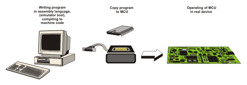
The end or...?
This section briefly describes the use of HT-MC02 and programmer software developed by FlashMagic. Everything is very simple...
 Start the program Keil IDE. The window appears...
...Open a new document: File -> New. Write your program or copy text...
... Save and name your document: File -> Save As... (Document name is limited to 8 characters!)
Finally, to compile program into HEX code select: Project -> Build or click the 'play' icon.
If everything works properly, the computer will respond with a short report.
The program is written and successfully compiled. All that's left is to dump the program to the microcontroller. For this purpose it is necessary to have a software that takes the written and compiled program and passes it to the microcontroller.
Start the program 8051 Flash_setup.exe...
Program installation is performed as usually - just click Next, Accept, Next...
...and finally - Finish
The program has been installed and ready for use. The settings are easily performed so that there is no need for additional explanations (the type of the microcontroller, frequency and clock oscillator etc.).
- Connect the PC and programmer via a USB cable;
- Load the HEX code using command: File -> Load HEX; and
- Click the 'Write' push button and wait...
Development Systems
A device which in the testing program phase can simulate any environment is called a development system. Apart from the programmer, the power supply unit and the microcontroller’s socket, the development system contains elements for input pin activation and output pin monitoring. The simplest version has every pin connected to one push button and one LED as well. A high quality version has LED displays, LCD displays, temperature sensors and all other elements which can be supplied with the target device. These peripherals can be connected to the MCU via miniature jumpers. In this way, the whole program may be tested in practice during its development stage, because the microcontroller doesn't know or care whether its input is activated by a push button or a sensor built in a real device.
7.2 HT-MC02 Development/Programmer Systems
The HT-MC02 development system is a high-quality development system used for programming 8051 compatible microcontrollers manufactured by NXP. In addition to chip programming, this system enables all the parts of the program to be tested as it contains most components which are normally built in real devices.
The HT-MC02 development system consists of:
- Sockets for placing microcontrollers in (14, 16, 20 and 40- pin packages)
- Connector for external power supply (DC 12V)
- USB programmer
- Power Supply Selector (external or via USB cable)
- 8 Mhz Quartz Crystal Oscillator
- 32 LEDs for output pin state indication
- 32 push buttons for input pin activation
- Four 7-segment LED displays in multiplex mode
- Graphic LCD display
- Alphanumeric LCD display (4- or 8- bit mode)
- Connector and driver for serial communication RS232
- Digital thermometer DS1820
- 12- bit A/D converter (MCP3204)
- 12- bit D/A converter (MCP4921)
- Reference voltage source 4.096V (MCP1541)
- Multiple-pin connectors for direct access to I/O ports
The following text describes in short some circuits within this development system. It is rather illustration of its features than complete manual. Besides, by learning about this device, one understands that microcontrollers and its tools are intended to everybody, not only to the privileged.
Why Program in C?
One advantage of using C to program microcontrollers is program portability. Each microcontroller has an individual instruction set and assembly language. Modifying assembly language code so a program written for one microcontroller will run on a different microcontroller is very time consuming and effort intensive.
Writing C code that supports general microcontroller features helps to avoid portability problems. Details relating to specific hardware implementations can be placed in separate library functions and header files. Using C library functions and header files ensures that application source code can be recompiled for different microcontroller targets.
C is a high level language. You will be able to program your applications quickly and easily using C. C’s breadth of expression is concise and powerful. Therefore, each line of code written in C can replace many lines of assembly language. Debugging and maintaining code written in C is much easier than in assembly language code.
- First Steps with Embedded Systems
- Memory Allocation In C

- C-Syntax Quick Reference
- An Introduction To The Use Of The Keil C51 Compiler
- Programming Embedded System in C (10 weeks Course)
 |
First Steps with Embedded SystemsThis book will be useful both as an introduction to microcontroller programming in C programming language for intermediate level post-secondary programs and as a guide for developers coping with the growth and change of the microcontroller industry.
|
 |
Quick Reference Guide for C languageThis reference guide is intended to quickly introduce user’s to C language syntax with the aim to easily start programming microcontrollers along with other applications. Why C in the first place? The answer is simple: C offers unmatched power and flexibility in programming microcontrollers. |
 |
An Introduction To The Use Of The Keil C51 Compiler On The 8051 FamilyThe Keil C51 compiler has been written to allow C programmers to get code running quickly on 8051 systems with little or no learning curve. To get the maximum performance from the 8051 family, knowing a few tricks is very useful... |
![]()