ACTIVE 3-WAY LOUDSPEAKER
Designing an active loudspeaker system is a complex (but fascinating) matter because each drive unit needs its own output amplifier and cross-over filter. But, of course, an active system has several advantages over a passive one. The present circuit, comprising three filter sections. active bass corrective network. and three output stages, fits on just one printed-circuit board.
Two of the advantages of an active loudspeaker system over a passive one are that neither loudspeaker cables nor a passive cross-over filter are required. The lack of loudspeaker cables saves money, too, since good quality ones are expensive. A passive filter dissipates energy in the inductors and capacitors. and this causes some deterioration in the quality of sound reproduction. An active filter uses no inductors and the capacitors have a much lower value, so that their quality can be of better quality. Moreover, in direct coupling there are no capacitors and inductors with loss resistances, and this means that the loudspeakers are under more direct control of the output stages.
Two of the drawbacks of an active system are its cost and higher complexity. These two go together, because it is the complexity of the electronic circuits (each loudspeaker needs it own output stage. for instance) that costs the money. In the present design. the output stages have been kept small through the use of modules for the medium and high frequency sections.
Some design considerations
The design (see block diagram) allows for various configurations of the crossover networks. The audio signal from the preamplifier is applied to the three filters (bass, medium and treble) via a buffer stage. Each of the filters may be given a rolloff of 6 dB. 12 dB or 18 dBper octave depending on the value of certain components.The low-pass filter is followed by a bass correction network. The original design of this network is due to Linkwitz. It is particularly useful to lower the response of the woofer in a closed box.
The formulas for the calculations of the correct component values and the rolloffs will be given later.
The outputs of the filters are applied to amplifiers. Note that the LF stage has more than twice the power output of the middle and high frequency one. Since the LF stage has been designed with discrete components. its output is applied to the drive unit via a power-on delay. This delay is an integral part of the medium and high frequency modules.
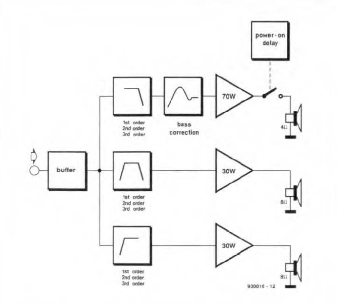 Fig. 1. Block diagram of the active 3-way loudspeaker system.
Practical design
Opamp IC2b (see Fig. 3) buffers the applied audio signal to prevent this being loaded unnecessarily. The input impedance is determined by R1. The output of IC2b is split three way to IC1a, IC1b and IC1c. Each of these circuits forms a third order filter, which may be converted into a first or second order type by omitting certain components. The middle-frequency section has two filters, IC1c, and IC1d, because it needs a rolloff at the low frequency end and one at the high frequency end. With values as shown, the cut-off frequencies are at 500 Hz and 500 Hz respectively. The response is a Butterworth type.
3-way_Amp_schFig-3: Circuit Diagram of the Active 3-Way Loud Speaker System.
It is possible to convert the present system into an active two-way one by omitting the entire middle-frequency section and the associated output stage (1C4). The low-pass filter is followed by the Linkwitz correcting network that matches the frequency response to the low cutoff point of the box. In this way, an octave is added to the lower portion of the response of the enclosure. It is. however. only possible to use the arrangement with boxes whose Qtc and fc are known. The calculations of the values of the network components are given later.
The supply voltages for the opamps are stabilized by IC6 and IC7. These voltages are derived from the ±25 V supply for the LF output amplifier (and for the other output stages if this is desired—more about this later).
Output modules IC4 and IC5 need only a few external passive components and a feedback loop. If the supply to them is ±25 V, they deliver an output of up to 30W into 8Ω. Noteworthy in the diagram of their internal circuitry, shown in Fig. 2, are the many protection circuits. Their input has a mute stage to prevent on and off switching becoming audible.
Concentrating on IC4, capacitor C26 prevents any d.c. components reaching the opamp. Low-pass filter R39-C27 limits the bandwidth of the input signal to a degree that is suitable for the output amplifier. The input impedance of that amplifier is determined by R43. The a.c. amplification of the module is set by feedback network R42-R41. The d.c. amplification is limited to unity by C28. Network R43-R44-C29 forms a bootstrap that increases the full power available from the output stage slightly. Boucherot network R45-C30 in parallel with the loudspeaker serves as load at high frequencies when the loudspeaker becomes inductive. Power-on delay is provided by R46–C31.
The presets between the filters and the loudspeakers serve to match the speakers as far as efficiency is concerned .
The LF output stage is a semi-discrete design to obtain a higher power since human hearing is less sensitive to low frequencies. The board has been designed to enable this amplifier operating from a power supply different from that for the middle and high frequency stages.
The supply for the differential input opamp. IC3, is derived from the main supply via networks R31-D3 and R32-D4. The input impedance of the opamp is determined mainly by R12. The bandwidth of the input to the opamp is limited by R11-C9. R15~C10 is a compensating network.
The output of IC3 is applied to a compound output stage, which provides not only current amplification, but also voltage amplification. This allows the opamp, although its output is limited by the ±20 V supply, to fully drive the power stage, whose supply is ±25 V.
The output stage consists of T4-T5 for the positive half of the signal and T6-T7 for the negative half. The power stage is driven by IC3 via two current sources, T1-D1 and T2-D2. The quiescent current through the output stage is determined by T3. which functions as a variable zener diode. The overall feedback is provided by R13 and R14.
The relay contact at the output of the low-frequency power stage prevents on/off clicks becoming audible. At power on. the relay is energized after a delay by T8 and T9. Before T9 can conduct, C15 needs to be charged via R29 and D7 to a voltage of 2.7 V (D6) plus 0.6 V (base- emitter junction of T9). Diode D7 ensures that the relay is de-energized immediately the supply voltage is switched off.