- 1. Introduction
- 2. How Class-D Works
- 3. Topologies
- 4. Gate Driving
- 5. Level Shifting
- 6. Output Filter Design
- 7. Feedback
- 8. Other Topologies
- 9. Some Final Note
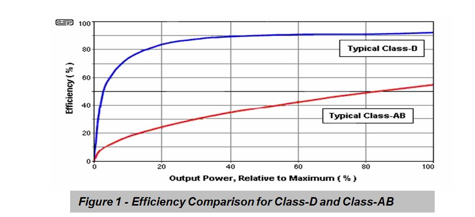
A completely new technology for audio amplification has been evolving during the last 15-20 years that has a clear benefit over current widespread Class-A, and AB topologies. We are talking about the so-called "Class-D". This benefit is mainly its high power efficiency. Figure 1 shows typical efficiency curves vs. Output power for Class-B and Class-D designs.
The theoretical maximum efficiency of Class-D designs is 100%, and over 90% is attainable in practice. Note that this efficiency is high from very moderate power levels up to clipping, whereas the 78% maximum in Class-B is obtained at the onset of clipping. An efficiency of less than 50% is realised in practical use with music signals. The PWM amp's high power efficiency translates into less power consumption for a given output power but, more important, it reduces heat-sink requirements drastically. Anyone who has built or seen a high-powered audio amplifier has noticed that big aluminium extrusions are needed to keep the electronics relatively cool. The loading on the power transformer is also reduced by a substantial amount, allowing the use of a smaller transformer for the same power output.
These heat-sinks account for an important part of the weight, cost and size of the equipment. As we go deeper in the details of this topology, we will notice that a well behaving (low distortion, full range) Class-D amplifier must operate at quite high frequencies, in the 100KHz to 1MHz range, needing very high speed power and signal devices. This has historically relegated this class to uses where full bandwidth is not required and higher distortion levels are tolerable - that is, subwoofer and industrial uses.
However, this has changed and thanks to today's faster switches, knowledge and the use of advanced feedback techniques it is possible to design very good performance Class-D amplifiers covering the whole audio band. These feature high power levels, small size and low distortion, comparable to that of good Class-AB designs. (From now on, we will refer to Class-A and AB topologies as "classical").
 From the DIY perspective, Class-D is rather unfortunate. Because of the extremely high switching speeds, a compact layout is essential, and SMD (surface mount devices) are a requirement to get the performance needed. The stray capacitance and inductance of conventional through-hole components is such that it is almost impossible to make a PWM amplifier using these parts. Indeed, the vast majority of all ICs used for this application are available only in surface mount, and a look at any PWM amplifier reveals that conventional components are barely used anywhere on the board. Since SMD parts are so hard to assemble by hand and the PCB design is so critical to final performance, DIY versions of PWM amps are very rare indeed.
In classical amplifiers, at least one of the output devices (let them be bipolar transistors, MOSFETs or valves) is conducting at any given time. No problem so far, but they are also carrying a given current where there is a voltage drop between collector-emitter / drain-source etc. Since P = V * I, they are dissipating power, and even if there is no output a small quantity of current must pass through the transistors to avoid crossover distortion, so some dissipation is present. As the output voltage increases, for given supply rails the voltage drop across the transistors will fall, but the current increases. At saturation (clipping), VCE or VDS will be low, but current is quite high (Vout / Rspk). Conversely, at low power levels, current is small but voltage drop is large. This leads to a power dissipation curve that is not linear with output power. There is a non-zero minimum dissipation (zero percent efficiency), and a point where maximum efficiency is reached ... about 78% in pure Class-B designs, 25% or less with Class-A.
Class-D on the other hand, bases its operation in switching output devices between 2 states, namely "on" and "off". Before discussing the topology specific details, we can say that in the "on" state, a given amount of current flows through the device, while theoretically no voltage is present from drain to source (yes, almost every Class-D will use MOSFETs), hence power dissipation is theoretically zero. In the off state, voltage will be the total supply rails as it behaves like an open-circuit, and no current will flow (that's very close to reality).
But how can our beloved audio signal be represented by an awful square wave with only two possible levels? Well, in fact it modulates some characteristics of this square wave so the information is there. Now we "only" have to understand the way the modulation is done and how to restore the amplified audio signal from it. The most common modulation technique used in Class-D is called PWM (Pulse Width Modulation) - a square wave is produced that has a fixed frequency, but the time it is in the "high" and "low" states is not always 50%, but it varies following the incoming signal. This way, when the input signal increases, the "high" state will be present for longer than the "low" state, and the opposite when the signal is "low". If we do some maths, the mean value of the signal in a single cycle is simply ...
Vmean = Vhigh * D + Vlow * (1-D), where D = Ton / T, (duty cycle)
T being the period of the signal, that is, 1/Fsw (switching frequency).
For example, the mean value of a 50% duty cycle (both states are present for exactly the same amount of time) signal going from +50V to -50V is: 50 * 0.5 + (- 50) * 0.5 = 0V. In fact, the idle (no signal) output of a Class-D amplifier is a 50% duty cycle square signal switching from the positive to the negative rail.
If we modulate the input up to the maximum, we will have a near-100% duty-cycle. Lets put 99%: Vmean = 50 * 0.99 + (-50) * 0.01 = 49V. Conversely, if the signal is lowest, we need near 0% (lets use 1%), so Vmean = -49V.
PWM is usually generated by comparing the input signal with a triangle waveform as shown in Figure 2. The triangle wave defines both the input amplitude for full modulation and the switching frequency.
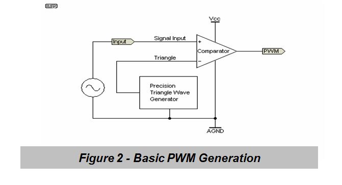
Figure 3 shows a typical PWM signal modulated by a sine wave. Notice that it is designed so signals between -1 and 1V will produce 0% to 100% duty cycles, 50% corresponding to 0V input. The 'digital' output uses standard logic levels, where 0V is a logic '0' and 5V is a logic '1'. Because of this digitisation of the signal, PWM amps are sometimes erroneously referred to as digital amps. In fact, the entire process is far more analogue than digital.

Notice that for a correct representation of the signal, the frequency of the PWM reference waveform must be much higher than that of the maximum input frequency. Following Nyquist theorem, we need at least twice that frequency, but low distortion designs use higher factors (typically 5 to 50). The PWM signal must then drive power conversion circuitry so that a high-power PWM signal is produced, switching from the +ve to -ve supply rails (assuming a half-bridge topology).
The spectrum of a PWM signal has a low frequency component that is a copy of the input signals spectrum, but also contains components at the switching frequency (and its harmonics) that should be removed in order to reconstruct the original modulating signal. A power low-pass filter is necessary to achieve this. Usually, a passive LC filter is used, because it is (almost) lossless and it has little or no dissipation. Although there must always be some losses, in practice these are minimal.
There are basically two Class-D topologies - half-bridge (2 output devices are used) and full-bridge (4 output devices). Each one has its own advantages. For example, half-bridge is obviously simpler and has more flexibility as a half-bridge amplifier can be bridged as with classical topologies. If it is not correctly designed and driven, can suffer from "bus pumping" phenomena (transfer current to the power supply that can make it increase its voltage producing situations dangerous to the amplifier, supply and speaker).
Full bridge requires output devices rated for half the voltage as an half bridge amplifier of the same power, but it is more complicated. Figures 5a and 5b show both topologies conceptually. Obviously, many components such as decoupling capacitors, etc are not shown.
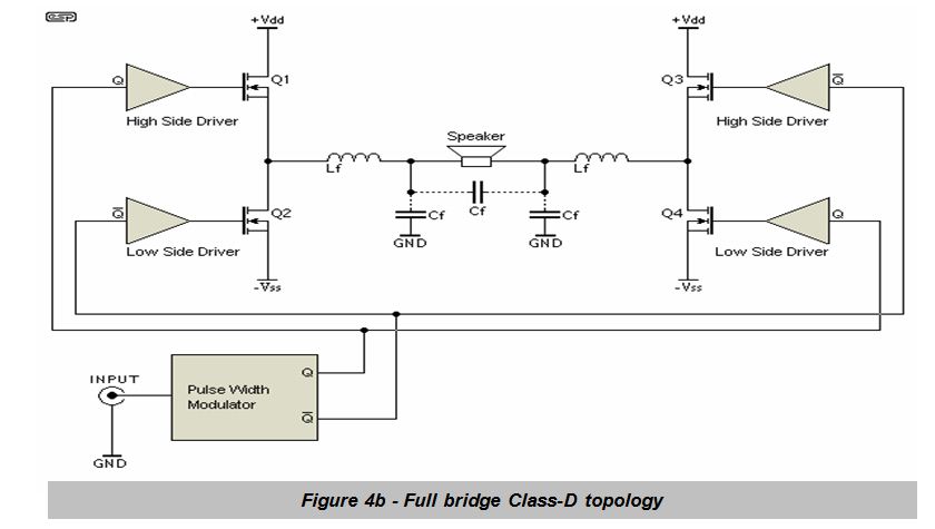
Note that full bridge PWM amp needs only one supply rail - bipolar supplies are not necessary, but can still be used. When a single supply is used, each speaker lead will have ½ the Vdd voltage present. As it is connected differentially, the loudspeaker doesn't see any DC if everything is well balanced. However, this can (and does) cause problems if a speaker lead is allowed to short to chassis! The filter may be implemented by means of a single capacitor across the loudspeaker, by a pair of caps to ground, or in some cases by both (as shown by the dotted lines connecting the caps).
For the rest of the document, we will concentrate on half-bridge topologies, although the vast majority of the ideas are also applicable to full-bridge designs.
Half bridge design
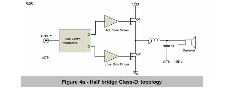
The operation of the half bridge circuit depicted in Figure 4a is as follows:
When Q1 is on (corresponding to the positive part of the PWM cycle), the switching node (inductor input) is connected to Vdd, and current starts to increase through it. The body diode of Q2 is reverse biased. When Q2 is on (negative part of the PWM cycle), the body diode of Q1 is reverse biased and the current through Lf starts to decrease. The current waveform in Lf is triangular shaped.
Obviously, only one of the transistors must be on at any time. If for any reason both devices are enhanced simultaneously, an effective short-circuit between the rails will be produced, leading to a huge current and the destruction of the MOSFETs. To prevent this, some "dead-time" (a small period where both MOSFETs are off) has to be introduced.
Lf in conjunction with Cf and the speaker itself form the low pass filter that reconstructs the audio signal by averaging the switching node voltage.
Timing is critical in all this process: any error as delays or rise-time of the MOSFETs will ultimately affect efficiency and audio quality. So all the involved components must be high-speed. Dead-time also affects performance, and it must be minimised. At the same time, the dead-time must be sufficiently long to ensure that under no circumstance both MOSFETs are on at the same time. Typical values are 5 to 100ns.
The dead-time is a critical factor for distortion performance. For lowest distortion, the dead-time must be as small as possible, but this risks 'shoot-through' currents, where both MOSFETs are on simultaneously. This not only increases distortion and dissipation dramatically, but will quickly destroy the output devices. If the dead-time is too great, the response of the output stage no longer follows the true PWM signal generated in the modulator, so again distortion is increased. In this case, dissipation is not affected.
To ensure fast rise/fall times of the MOSFETs, the gate driver must provide quite a high current to charge and discharge the gate capacitance during the switching interval. Typically, 20 - 50ns rise/fall times are needed, requiring more than 1A of gate current.
Note that the schematics shown use both N-channel MOSFETs. Although some designs use N and P channel complementary devices, that is IMHO sub-optimal due to the difficulty of obtaining suitable P devices and matched pairs. So lets concentrate on N-channel only half-bridges. Note that, in order to drive a MOSFET on, a voltage above Vth must be present between its gate and source. The lower MOSFET has its source connected to -Vss, so its drive circuit has to be referred to that node instead of GND.
However, the upper MOSFET is more difficult to drive, as its source is continuously floating between +Vdd and -Vss (minus drops due to on resistance). However, its driver must be also floating on the switching node and, what's more, for the on-state, its voltage must be several volts above +Vdd so a positive Vgs voltage is created when Q1 is on. This also implies a voltage shifting so the modulator circuit can communicate correctly with the driver.
This is one of the major difficulties of Class-D design: gate drive. To solve the issue, several approaches are taken ...
- Transformer gate drive: useful in half-bridge power supplies where duty-cycle doesn't vary widely. In audio amplifiers however, duty cycle ranges from 0% to 100%, so this method creates a problem because the signal is AC coupled. A DC restoration circuit (not shown) is needed.
- Discrete gate driving: some designs use transistors to perform both the level shifting and the MOSFET drive. Again, there is a problem: we need a voltage that is higher than +Vdd.
- Integrated drivers: there are a number of MOSFET drivers in the market, optimised for high speed, that can be used. Again, a voltage higher than Vdd is needed as well as level shifting.
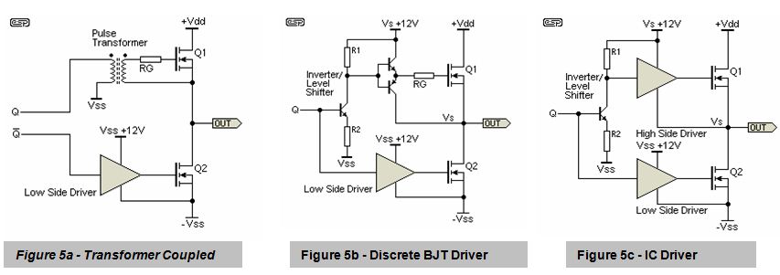
Note that circuits in figures 5b and 5c have their PWM input referred to -Vss so may require previous level shifting of the comparator output, that will normally be referred to GND. Fig 5a will require level shifting of the inverted PWM only, as the transformer input can be referenced to GND as shown. Many of the driver ICs available now have inbuilt level shifters, and these are optimised for speed. Remember that any delay introduced into the switching waveform can cause distortion or simultaneous MOSFET conduction.
We have still one problem to solve ... obtaining 12V above VS (the switching node). We can add another power supply, isolated from the main one, which (-) is connected to VS. This solution can be impractical, so other techniques are commonly used. The most widespread is a 'bootstrap' circuit. The bootstrap technique uses a charge pump built with a high speed diode and a capacitor. The output of the amplifier produces the switching pulses needed to charge the capacitor.
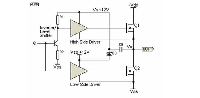
This way, the only auxiliary power supply needed is 12V referenced to -Vss that is used for powering both the low side driver and the charge pump for the high side driver. As the average current from this supply is low (although there are high current charging peaks during the switching events, they last only 20-50ns, twice during a cycle, so the average is quite low, in the 50-80mA range), this supply is easily obtained from the negative rail with a simple 12V regulator (paying attention to its maximum input voltage rating, of course).
As can be seen from the previous figures, in order to excite the MOSFET driver, the PWM signal has to be referred to -Vss. So, as the modulator usually works from +/-5 to +/-12V, typically, a level shifting function is needed. One can choose to shift the level of the PWM signal and then generate the inverted version, or generate both outputs and invert both of them. It depends, for example, on the comparator type used (if complementary outputs are available, the decision is made).
A basic level shifting function can be performed with a single or two-transistor circuit similar to the one depicted in Figure 6 (before the high side driver). While this may work at low frequencies, it is important to simulate the behavior of the comparator and level shifter, as they can introduce considerable delays and timing errors if not properly designed.
It is fair to say that the level shifter is one of the most critical parts of the circuit, and this is evidenced by the wide variety of competing ICs designed for the job. Each will have advantages and disadvantages, but in all cases the complexity is far greater than may be implied by the simplified diagrams.
The output filter is one of the most important parts of the circuit, as the overall efficiency, reliability and audio performance depends on it. As previously stated, a LC filter is the common approach, as it is (theoretically) lossless and has a -40dB/decade slope, allowing for a reasonable rejection of the carrier if the parameters of the filter and the switching frequency itself are properly designed.
The first thing to do is to design the transfer function for the filter. Usually, a Butterworth or similar frequency response is chosen, with a cutoff frequency slightly above the audio band (30-60KHz). Have in mind that one of the design parameters is the termination load, that is, the speaker impedance. Usually, a typical 4 or 8 ohm resistor is assumed, but that would produce variations in the measured frequency response in presence of different speakers. That must be compensated for by means of proper feedback network design. Some manufacturers simply leave it that way so the response is strongly dependent on the load. Surely a non-desirable thing.
The design can be done mathematically or simply use one of the many software programs available that aid in the design of LC filters. After that, a simulation is always useful. Figure 7 shows a typical LC filter for Class-D amplifiers and its typical frequency response.
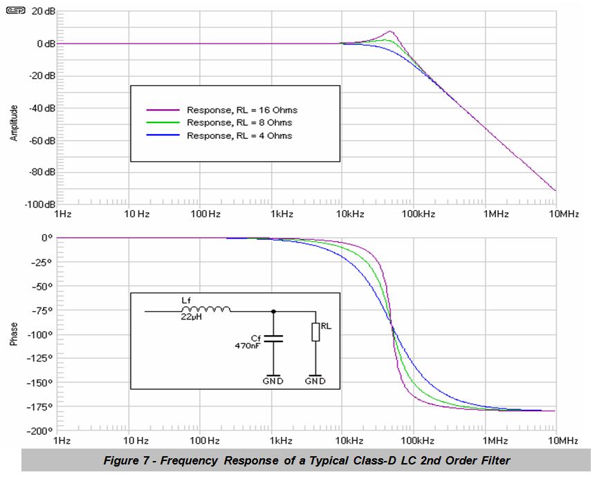
This simple filter has a -3dB cutoff frequency of 39KHz (with 4 ohm load), and suppresses the carrier as much as 31dB at 300KHz. For example, if our supply rails are +/-50V (enough for about 275W at 4 ohms), the residual ripple will have an amplitude of about 1Vrms.
This ripple is, obviously inaudible, and 1V RMS will dissipate only around 200mW in a typical tweeter (not likely a problem, especially since the tweeters impedance will be a lot higher than 8 ohms at 300kHz). However, care must be taken as the speaker wires can become an antenna and affect other equipment. In fact, although a couple of volts RMS of ripple can seem low enough to run your speakers safely, EMI can be a concern, so the less carrier level you have, the better. For further rejection, higher order filters are used (with the potential disadvantage of increased phase shift in the audio band), although there are other clever ways to do it, as very selective bandstop or 'notch' filters tuned to the carrier frequency (if it is fixed, and that only happens in synchronous designs as the one described).
Well designed Class-D amplifiers have a higher order filter and/or special carrier suppression sections in order to avoid problems with EMI. As can be seen in Figure 8, the response is dependent on the load, and in fact the load is part of the filter. This is one of the problems to solve in Class-D designs. It doesn't help that a loudspeaker presents a completely different impedance to the amplifier than a test load, and many PWM amps have filters that are (and never can be) correct for all practical loudspeaker loads. Again, only a handful of good Class-D amplifiers use feedback techniques that include the output filter to compensate for impedance variations and have a nearly load independent frequency response, as well as to reduce distortion produced by non-linearities in the filter. Although passive components are thought to be distortion-free, this does not apply to ferrite or powdered iron cores that are used for the filters. These components most certainly do introduce distortion.
Now, The Filter Components ...
The output inductor has to withstand the whole load current, and also have storage capability, as in any non-isolated switching converter (Class-D half bridge design is in fact analogous to a buck converter, its reference voltage being the audio signal).
The ideal inductor (in terms of linearity) is an air-core one, but the size and number of turns required for typical Class-D operation usually makes it impractical, so a core is normally used in order to reduce turns count and also provide a confined magnetic field that reduces radiated EMI. Powder cores or equivalent materials are the common choice. It can also be done with ferrite cores, but they must have a "gap" where energy is stored. Wire size must also be carefully chosen so DC losses are low (requiring thick wire) but also skin effect is reduced (AC resistance must also be low).
Inductor core shape can be a drum core, gapped ferrite RM core, or toroidal powder core, among others. Drum cores have the problem that their magnetic field is not enclosed, hence producing more radiated EMI. RM cores solve this problem but have most of the coil enclosed, so cooling problems may arise as no airflow is possible. IMHO, toroids are preferred because they feature both closed magnetic field that helps control radiated EMI, a physically open structure that allows proper cooling, and easy and economical winding, as they don't need bobbins.

As we have stated previously, timing errors can lead to increased distortion and noise. This cannot be skipped and the more precise it is kept, the better the design will perform. Anyway, open loop Class-D amplifiers are not likely to satisfy demanding specifications, so (negative) feedback is almost mandatory. There are several approaches. The most simple and common is to take a fraction of the switching signal, precondition it by means of a passive RC low pass filter and feed it back to the error amplifier.
To put it simply, the error amplifier is an op-amp placed in the signal path (before the PWM comparator) that sums the input signal with the feedback signal to generate a error signal that the amps automatically minimises (this is the concept of every negative-feedback system, anyway).

Although good results are obtained this way, there is still a problem: load dependency, due to the speaker being an integral part of the filter, hence affecting its frequency response as shown above.
Some more advanced amplifiers take the feedback signal from the very output, trying to compensate this. This way, a constant frequency response is obtained, with the further gain that the inductor resistance contributes much less to the output impedance, so it is kept lower, hence damping factor is higher (higher speaker control). However, taking feedback after the filter is not an easy task. The LC introduces a pole and hence a phase shift that, if not properly compensated, will make the amp become unstable and, ultimately, oscillate. Feedback may be taken from both the switching node and the filter output. Although this can give very good results, it is still difficult to maintain stability because of the phase shift through the output filter.
Pure PWM (based on triangle generators, also called 'natural sampling PWM') is not the only way to go in order to construct a Class-D amplifiers. Some other topologies have arisen, many of them based on auto-oscillation, where the hysteresis in the comparator and delays between the comparator and power stage can be taken into account to design a system that oscillates by itself in a somewhat controllable manner.
Although simpler, these designs have some disadvantages, IMHO. For example, the switching frequency is not fixed, but depends on the signal amplitude. This makes output notch filters ineffective, yielding higher ripple levels. Besides, when several channels are put together, the difference in switching frequency between them can produce audible beat tones that can become very annoying. This can also happen of course with synchronous design as the one described here, but there is a simple solution - use the same clock for all the channels.
Self oscillating designs in particular have some other difficulties like start-up: special circuitry may be needed that forces the amplifier to start oscillating. Conversely, if for any reason the oscillation stops, you could end up with an 'always-on' MOSFET, and thus a large amount of DC at the output, followed almost immediately by a dead loudspeaker. Of course, these issues can be solved with proper design, but the added complexity can void the initial simplicity, thus no gain is obtained.
Low distortion in a PWM amplifier requires a very linear triangle waveform, along with a very fast and accurate comparator. At the high operating frequencies needed for optimum overall performance, the op-amps used need to have a wide bandwidth, extremely high slew rate, and excellent linearity. This is expensive to achieve, requiring premium devices. Some of these constraints are relieved somewhat by self oscillating designs (therefore making them slightly cheaper), but this is not an effective trade-off for the most part.
Clocked designs (fixed frequency) are not easier to make than self-oscillating or modulated switching frequency designs, but are certainly far more predictable and tend to have fewer problems overall. The ability to synchronise multiple amplifiers ensures that mutual interference is minimised. An 'advantage' claimed by the proponents of non-clocked and 'random switching' designs is that the RF energy on the speaker leads is spread over a wide frequency range, potentially making such amplifiers more likely (or perhaps less unlikely) to pass EMI testing. From an overall perspective, this is more likely to be a hindrance than a benefit, as it is no longer possible to optimise the filter network for maximum switching frequency rejection.
There are also PWM amps that claim to be truly 'digital', using One-Bit™ technology, or generating the PWM signal directly from the PCM data stream. Although the manufacturers of such amplifiers will naturally proclaim their superiority over all others, such self-praise should generally be ignored. Implementing feedback in a 'pure' digital design is at best difficult, and may be impossible without using a DSP (digital signal processor) or resorting to an outboard analogue feedback system. Including additional ADCs and DACs (analogue to digital converters and vice versa) is unlikely to allow the amplifier to be any 'better' than the direct analogue methods described in this article.
A relative newcomer to the scene is the Sigma-Delta modulator, however at the time of writing this still has problems (challenges in corporate speak). The main issue is that the transition rate is too high, and it must be reduced to accommodate real-world components - particularly the power switching MOSFETs.
The 'pure' digital solutions described above have another shortfall, and that's the fact that the number of different pulse widths is finite, and determined by the clock speed. A digital system can only switch on a clock transition. Based on currently available information, only around 8 x oversampling is possible if a digital noise shaping filter is added to the system. An analogue modulation system has an effectively infinite number of different pulse widths, but this is not possible with any true digital implementation.
These latter comments cover a very complex area, one is outside the scope of this article. However, even the scant information above will give most readers far more information that is commonly available - especially from manufacturers of digital Class-D amplifiers.
In conclusion, Class-D amplifiers have evolved a lot since they were first invented, achieving levels of performance similar to conventional amplifiers, and even better in some aspects, like an inherent low output impedance that allows effortless bass. All this, with the great advantage of high efficiency. Of course, only if they are properly designed.
However, although very attractive, Class-D designs are not very DIY friendly. In order to achieve a properly working design in terms of efficiency, performance and EMI, very careful PCB layout is mandatory, some component selections are critical and of course proper instrumentation is absolutely required.
This article has been written in order to throw some light about the internals, advantages and difficulties of this not very well-known (and even less well understood) technology. Everyone thinks that "Class-D" stands for "Digital". We hope that after reading this article, no-one thinks that any more.
- Download this application note in pdf.
- TDA7498 2x100W Class-D Audio Amplifier Board
- GPD2856C-MP3 Player Board
- VS1053B MP3/WAV/AAC/WMA Arduino Audio Shield


