The more resistance the better!
A timer circuit that turns on a pump for a short time every five minutes can be easily made using the famous 555 IC. Unfortunately, it’s almost impossible to avoid using electrolytic capacitors to achieve such a long period, which makes the circuit less accurate and reliable, especially in the longer term. However, there is one solution to this problem, and that is to use a special 1 giga-ohm resistor!
The circuit described here stands out by the fact that no electrolytic capacitors have been used for the components that determine the delay. Instead, ordinary film capacitors were used, which have a much lower leakage current than electrolytics. Since the capacitance of this type of capacitor is much lower than that of electrolytics with a similar size, the load resistor has to be a very high ohmic type. In this circuit a resistor of 1 GΩ (giga-ohm) is used! Most electronics hobbyists probably don’t even realize these exist. This component
appears to be available cheaply, it is a nice challenge to use it in the design for the timer.
Circuit without electrolytics
The result can be seen in Figure 1 and requires little explanation. There are two timers, which are connected in series. The first timer (IC1A) is configured as an astable multivibrator, with a period of about 270 s. The components R1, R2 and C1 are used to set this time. By using the previously mentioned 1GΩ resistor for R1, it is sufficient to use a capacitor of only 0.39μF to achieve this period. The second timer (IC1B) has been implemented as a monostable multivibrator.
With the component values given for R3 and C2 it outputs a positive pulse of about 7s when it gets a falling edge from the output of IC1A. The MOSFET (T1) is turned hard on during this time, powering the motor (max. 12V, 10A). The timer section can be switched on or off using switch S1, or it can be permanently activated via JP1. The pushbutton (S2) offers the facility to turn on the motor manually, and to keep it running for as long as the push button is held down. Finally, the power input is protected by a combination of a
resistor (R4) and a 12V zener diode (D1). These ensure that the timer circuit won’t be damaged by voltage spikes on the power input, or when the input voltage is a bit higher than 12V.
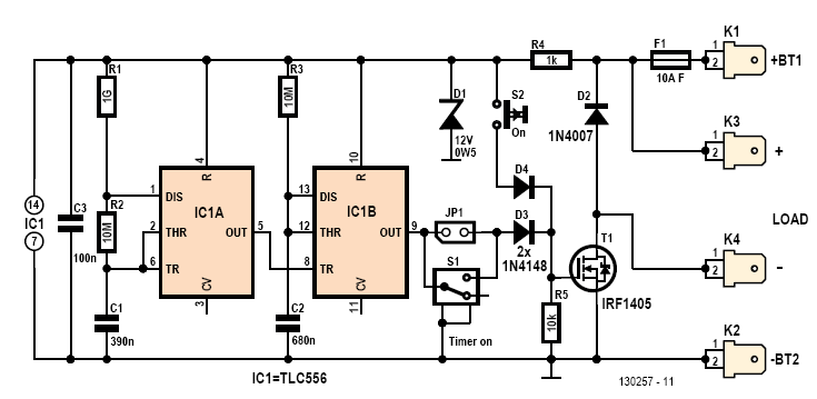
Figure 1.The circuit diagram for the timer circuit is straightforward. The most noticeable component is R1, a resistor with a value
of 1 GΩ.
Sturdy board
A small, single-sided printed circuit board without wire links has been designed for this circuit (Figure 2), measuring 58.2×43.6mm. It is very easy to build the circuit, since only through-hole mounted components have been used. A large area of the PCB has been taken up by the fuse and the ‘Faston’ spade terminals. The tracks on the PCB have been designed to cope with currents of up to 10A. The specified fuse holder clips (see parts list) can even cope with 15A. When switching currents up to 10A it is not necessary to mount MOSFET T1 on a heatsink, but we would recommend that you leave a gap of a few millimeters between the MOSFET and the PCB. This will prevent the specified Rth(j-a) from increasing too much (the PCB material underneath the FET would otherwise act as a thermal insulator). At a constant current of 10A the temperature of the FET rises to about 40°C above the ambient temperature (with UGS > 10V). This may seem like a lot, and it does feel hot, but the junction temperature will still be within its safe range. The MOSFET can also be mounted vertically, but this doesn’t make a lot of difference to its heat loss. The switch (S1) is mounted at the edge of the PCB. When the PCB is mounted in an enclosure the switch can still be operated through a small hole in the side of the case. The circuit can be permanently activated via a wire link or jumper across JP1 (obviously only as long as power is applied). Alternatively, you can solder two wires onto JP1 and connect them to an external switch, instead of using switch S1.
 Figure 2. The circuit board is single-sided, with the tracks for the switch section being suitable for currents up to 10 A.
Practical considerations
The measured period of IC1A in the prototype built was initially found to be over 20% longer (333s) than the theoretical value of 275.7s from:
T = C1 (R1+2R2) ln2 [s]
Even when we take all tolerances into account, we have to conclude that there are some parasitic resistances in the circuit. The combined bias currents of the threshold and trigger inputs (typically 20pA) only play a minor role in this. It turns out that it was caused mainly by contamination of the PCB and the 1GΩ resistor. To prevent this, you have to carefully handle R1 at all stages of the soldering, and clean the PCB on completion of the soldering. You should never touch the body of the 1GΩ resistor, as it will leave some grease from your skin behind. Only touch the end of the leads that will later be cut off. You should also mount the resistor slightly above the PCB, so it doesn’t make contact with the board. The current consumption of the circuit depends very much on the supply voltage. At 12V the circuit uses only about 300 μA. At higher voltages the zener diode (D1) will start to conduct, which increases the current consumption significantly (at 13.6V it goes up to 1.7mA). This won’t make any difference when you’re using a large lead acid battery as the power source, but in other applications this could be something you have to keep an eye on. If necessary, you could increase the zener voltage to 14V or 15V (the TLC55 is rated for use with supply voltages up to 18V). With a lower supply voltage (less than 10V), it is recommended that you limit the current to be switched. The ON resistance of T1 increases with a lower gate-source voltage, which increases the heating significantly. In this case, you will need to add a heatsink.
COMPONENT LIST
| R1 = 1GΩ 0.25W 10% | R2,R3 = 10MΩ | R4 = 1kΩ | R5 = 10kΩ |
| C1 = 390nF | C2 = 680nF | C3 = 100nF | D3,D4 = 1N4148 |
| D1 = BZX79-C12 Zener diode | D2 = 1N4007 | T1 = IRF1405ZPBF | IC1 = NE556N |