Moving signs are a common enough sight today but off-the-shelf units are invariably expensive and somewhat inflexible. The six-character module described in this article can be cascaded up to 16 modules long and has a character set that can be customised to suit your application.
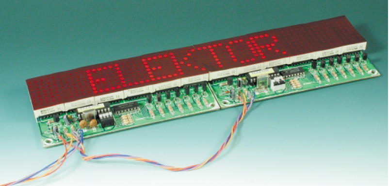
The dot matrix moving sign module presented here has a six character display area. A maximum of 16 of these modules can be cascaded together to produce a 96-character display. The PCB layout for the module can accommodate 5×7-Matrix displays with a distance between the rows of pins of 33.0 mm (30 mm character height) but larger or smaller displays may also be fitted by using adapter boards, if the LED matrix is electrically compatible, of course.
The big advantage of building this moving sign yourself is that the cost of the finished article is much less than that of a ready-built unit. Most of the ICs used in the design are widely available and relatively cheap. The passive components are all standard and an AT89C2051 with flash-memory is not the most expensive microcontroller. The main item from a cost point of view is the type of LED matrix displays that are used.
The microcontroller that controls the display module has a character set of 95 characters. The pre-programmed controller is supplied with the standard character set containing punctuation marks, symbols, numbers and the alphabet (in upper and lower case) but there is also the possibility to program your own special characters and implement simple graphics.

Figure 1. The circuit diagram of a dot-matrix module.
Display Multiplexing
A separate 5-V mains unit supplies power for this module. Each displayed character is made up of a 5×7 or 8×8 LED matrix. Assuming that each LED requires a current of 10mA, this gives us a worst case current consumption of 350mA or 640mA for each character. Multiplying this value by six for the six characters of each module may cause fear for a hefty power supply. In order to reduce the current required for the module — and to simplify the hardware and wiring necessary to drive the LEDs — this design uses multiplexing. This technique switches on the driver transistor for each horizontal row of LEDs in the matrix sequentially. If the lines are switched quickly enough then your eye will not see the flickering and they will appear to be continuously lit. The trade-off is that because each row of the character is only on for one seventh (in practice less) of the time that it would be if it were continuously lit, the display will not appear as bright. In practice the LED driver must also be blanked while each new row of information is shifted into the display shift registers. To offset the reduction in display brightness the LED current has been increased.
Looking at the circuit diagram shown in Figure 1 it can be seen that the column information for the display LEDs is supplied by the outputs of the six shift register ICs type 74LS164. Only five outputs are used on each shift register. The seven display matrix rows are selected by the three outputs of the microcontroller (P1.0 to P1.2) which control a one-of-eight decoder type 74LS138 (IC2). Two port
lines from the microcontroller control the shift registers. Port 1.7 is the data signal while P1.6 produces the clock signal. The reset inputs to the shift registers are not used — in this application it would have the effect of turning on all the LEDs in the matrix.
The display process begins by the controller selecting the ’invalid’ line 8 output of the display line driver (IC2). The effect of this is to turn off all the LEDs. This is necessary to blank out the passage of serial data through the shift registers which would otherwise cause all the LEDs to flicker dimly. The microcontroller will take the ASCII code of the character to be displayed from its internal memory and uses this value to access its corresponding display pattern in a character generator. The controller will then take the first line of the display pattern and send it out serially to the display shift registers. Any bit in the pattern that is ‘1‘ will turn the LED off, any bit that is a ‘0‘ will turn the LED on. The controller also generates the clock to transfer this serial data into the shift registers. This process is repeated for the first line of the other five display characters. After this the transistor driving the first row (R1) is enabled. All of the shift register outputs that are low will cause these LEDs in the first line to light for a short period until the row driving transistor is turned off. The same process is now repeated for the second row up to the seventh when the whole process is repeated. This is repeated until the PC sends a new character.
The circuit design
Looking at the details of the circuit we can see that the row addressing is performed by the 74LS138 (IC2) with active low outputs. PNP Transistors T2 to T8 are switched on when one of the outputs of IC2 goes low. Each transistor collector is connected to the anodes of a complete row of LEDs while the outputs of the shift registers (IC3 to IC8) are connected via current limiting resistors to the cathodes of each column of LEDs. These LS series shift registers should be capable of sinking 8-10mA on their outputs.
The LED dot matrix displays suggested for this design (Kingbright TC12-11 range) certainly produce the neatest finished product and also guarantee close matching of the LED‘s brightness. The Kingbright TC12-11HWA is stocked by Conrad Electronics and can be ordered from www.conrad-electronics.com. Unfortunately they are not really intended for multiplex operation. The light intensity of the LEDs are rated at 560–1400 μcd which is quite low. Even if the drive current is increased to 40mA we only achieve a doubling of the brightness. The value of the current limiting resistors R8 to R37 can be reduced to 220 Ω if the display is not bright enough for your application. RS components stock the excellent hyper red matrix type TC12-11SRWA currently priced at £6.14 each and they can be ordered on-line from www.rswww.com from their Electromail subsidiary. Kingbright also produce LED matrix’s in the same series with differentcolours but these may be difficult to obtain in small quantities:
TC12-11 Light intensity colour
μcd (IF=10 mA)
min – typ.
HWA 560-5600 Red
YWA 2200-5600 Yellow
SGWA 3600-9000 Green
EWA 3600-9000 Super red
SRWA 5600-14000 Hyper red
Another alternative is to make up your own LED matrix using individual LEDs. It is advisable to use ‘low current‘ types as these will emit the same light intensity at 2 mA as a standard LED at 10 mA. The main disadvantage of this method is the time and patience needed to solder all the LEDs to form an accurate matrix.
Each display module has its own address. A four-way DIP switch (S1) defines the binary coded address of the module (0 to 15) and is read by the controller at port pins P3.2 to P3.5. The serial data line from the PC is connected in parallel to each module and this switch setting is used by the controller on each module to ensure that only the correct part of the message is used by that module. The LSB switch position of this address is between pins 1 and 8 of S1 and each contact is closed when the slider on the top of the switch is nearest IC1 (assuming that you have mounted S1 the right way round).
The RS232 interface is a little unconventional in that it does not use the ubiquitous MAX232 interface chip. In this application data flows in one direction only so a simple transistor is used as the most economical solution. Input resistor R7 is used to limit the input current when the PC drives the data line high. Diode D1 limits the negative input voltage at the transistor to approximately minus 0.7V when the data line is driven low. Transistor T1 inverts the signal on the data line and applies it to input port 3.0 of the microcontroller.
This design operates without any handshaking protocol between the PC and the display module, but it is still necessary to connect the unused pins of the COM port to the correct signal levels so that the PC knows that the module is always ready to receive data. Some PCs are fitted with a 25-pin connector while others have a 9-pin. For those with a 25-pin connector it is necessary to link pin-4 with pin 5 and also to link pins 20, 6 and 8. For those with 9-pin connectors it is necessary to link pin 7 with pin 8 and also to link pins 1, 4 and 6
(see Figure 2).

Communication from the PC to the module takes place at 9600 baud, with no parity bit, 8 data bits and one stop bit. The microcontroller clock is supplied by a standard 22.1184 MHz crystal (X1). Other crystals can be used but this would require a change to the initialisation routine of the microcontroller. The complete module is powered from a single 5 V power supply. The LS-TTL chips used in the circuit consume almost 200 mA in their quiescent state. The LEDs will take approximately 10 mA each and because of the multiplexing only 30 LEDs (maximum) will be lit at any one time this gives a current of 300 mA. Adding this value to the 200 mA required for the control circuitry
we arrive at a current supply of 500 mA at 5 V.
Figure 3 shows the layout of the PCB. We have not tried to cram everything into the smallest space, the components are placed to simplify construction. The PCB is not double-sided so there are seven wire links to be placed on the circuit. The shift registers (IC3 to IC8) are mounted directly under the matrix LEDs so it is important to fit them
carefully to the PCB without using sockets. Sockets should however be used for all the remaining IC’s and the LED matrix chips themselves. As always, make sure that you give the finished board a thorough visual inspection after you have soldered all the remaining components to the PCB.
The Controller Software
The microcontroller mounted on the display module requires a program to receive the display information from the PC and to control the hardware. The software is available as a free download from the Elektor Electronics web site at www.elektor-electronics.co.uk. Along with the fully commented Assembler source code there is also the hex file ready to send to your device programmer. The controller is available pre-programmed from Elektor Electronics for those constructors who do not need to ‘tweak‘ the code in any way or do not have the means to program a chip themselves.

The controller software begins by initialising the stack pointer, the received serial data register and the timer register. The PBE routine is performed once during initialisation and reads the value of the DIP switch to find out the address of the module. An arithmetic and logic calculation is performed to work out the position of the characters in the received data stream that are intended for this module. The next five characters are loaded similarly into the memory. The LOE routine clears the display by sending out a series of 1‘s in the data stream that will turn off the outputs to the shift registers and also put an invalid address on the input of IC2. This has the effect of turning off the entire row driver transistors. The counter register that is used to unload the serial data from the PC is reset and the registers holding the display characters are cleared to ensure that they do not contain any random information. After resetting the hardware the display will have a blank display and the module will be ready to accept display characters over the serial interface from the PC. When ASCII characters arrive at the controller, the SERIN interrupt routine will be started. The first character is temporarily saved to a register and after incrementing the receive character counter the character is checked to determine if it is the control character $0C (form feed). If it is then we
jump to LOE where the display will be cleared and the receive character counter reset. Another test is performed in SER0 to check if the received character is greater than $20 any character less than this is invalid and would cause the character generator table pointer to point to a program code address rather than the character generator table resulting in a invalid display pattern. Other methods of character generation are too processor intensive and cause the display to flicker. SER1 tests if the received character is intended for this display position and checks that the address of the module calculated in the PBE routine, if there is no match then the routine will be exited and only the character counter will be incremented. The character will only be loaded into the register to be displayed if it is intended for this position and less than $20.
 After receiving and checking the ASCII code for the character it will be converted into the correct display pattern. A program loop calculates the information of each display row from the ASCII character and the character generator table and stores it in register A. The ANZ routine shifts the character row information serially into the shift registers and also generates the clock. This process is repeated for each of the six display registers R2 to R7.
When a complete row is loaded to all of the shift registers, the line driver transistor will be switched on by sending the binary code corresponding to the line number to IC2. After this display period, the ’invalid’ address code of $08 is sent to IC2 this will switch off all of the transistors. The next line will now be sent to the shift registers and this will continue for all of the seven rows of the display. The whole process is then continually repeated from the start.
The PC Software
If we take a look at the other end of the RS232 cable we can see that we need a PC running some sort of terminal program. This type of program will convert the characters to be displayed into ASCII and send them serially over the cable. Your PC will be behaving just like a computer terminalrather than a stand-alone PC (hence the name of this type of program). A proprietary program such as HyperTerminal could be used but it is often more interesting and instructive to write your own routine. Figure 4 shows an example program written in BASIC, this outputs the character string contained between the quotes in the line beginning Z$ via the COM2 port of the PC. The message runs from right to left over two cascaded display modules. The part of the program named ‘output loop‘ contains a counter value (V) which indicates how many character positions there are in the module. The value in this output loop reflects the number of modules that are cascaded, this value is always a multiple of 6 and in this example with two modules the figure is 12: FOR ZA = V + 1 TO V + 12 For three modules this value would be 18, and so on. The value of ZT in the next part of the program is used to introduce a time delay that will control the speed of the characters moving across the display. A value of 50000 for this delay gives a reasonable appearance with our PC but if you are using a newer, faster machine it will be necessary to increase this value perhaps by a factor of ten or even one hundred. Finally, we should repeat that the DIP switch setting is only read at power-on.

![]()
Part List
Semiconductors:
| D1 = 1N4148 | LD1-LD6 = TC12-11SRWA | T1 = BC547 | T2…T8 = BC640 |
| IC1 = 89C2051-24PC | IC2 = 74LS138 | IC3-IC8 = 74LS164 |